HGTG40N60B3 Fairchild Semiconductor, HGTG40N60B3 Datasheet - Page 2
HGTG40N60B3
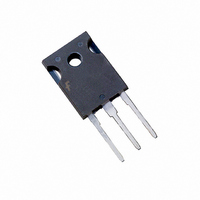
Manufacturer Part Number
HGTG40N60B3
Description
IGBT N-CH UFS 600V 70A TO-247
Manufacturer
Fairchild Semiconductor
Datasheet
1.HGTG40N60B3.pdf
(8 pages)
Specifications of HGTG40N60B3
Voltage - Collector Emitter Breakdown (max)
600V
Vce(on) (max) @ Vge, Ic
2V @ 15V, 40A
Current - Collector (ic) (max)
70A
Power - Max
290W
Input Type
Standard
Mounting Type
Through Hole
Package / Case
TO-247-3
Channel Type
N
Configuration
Single
Collector-emitter Voltage
600V
Collector Current (dc) (max)
70A
Gate To Emitter Voltage (max)
±20V
Package Type
TO-247
Pin Count
3 +Tab
Mounting
Through Hole
Operating Temperature (min)
-55
Operating Temperature (max)
150C
Operating Temperature Classification
Military
Transistor Type
IGBT
Dc Collector Current
70A
Collector Emitter Voltage Vces
600V
Power Dissipation Pd
290W
Collector Emitter Voltage V(br)ceo
600V
Operating Temperature Range
-55°C To +150°C
Rohs Compliant
Yes
Lead Free Status / RoHS Status
Lead free / RoHS Compliant
Igbt Type
-
Lead Free Status / Rohs Status
Compliant
Available stocks
Company
Part Number
Manufacturer
Quantity
Price
Company:

Part Number:
HGTG40N60B3
Manufacturer:
FAIRCHILD
Quantity:
12 500
Part Number:
HGTG40N60B3
Manufacturer:
HARRIS
Quantity:
20 000


Absolute Maximum Ratings
Collector to Emitter Voltage . . . . . . . . . . . . . . . . . . . . . . . . . . . . . . . . . . . . . . . . . . . . . .BV
Collector Current Continuous
Collector Current Pulsed (Note 1) . . . . . . . . . . . . . . . . . . . . . . . . . . . . . . . . . . . . . . . . . . . I
Gate to Emitter Voltage Continuous. . . . . . . . . . . . . . . . . . . . . . . . . . . . . . . . . . . . . . . . . V
Gate to Emitter Voltage Pulsed . . . . . . . . . . . . . . . . . . . . . . . . . . . . . . . . . . . . . . . . . . . .V
Switching Safe Operating Area at T
Power Dissipation Total at T
Power Dissipation Derating T
Reverse Voltage Avalanche Energy . . . . . . . . . . . . . . . . . . . . . . . . . . . . . . . . . . . . . . . . . E
Operating and Storage Junction Temperature Range . . . . . . . . . . . . . . . . . . . . . . . . T
Maximum Lead Temperature for Soldering . . . . . . . . . . . . . . . . . . . . . . . . . . . . . . . . . . . . . T
Short Circuit Withstand Time (Note 2) at V
Short Circuit Withstand Time (Note 2) at V
CAUTION: Stresses above those listed in “Absolute Maximum Ratings” may cause permanent damage to the device. This is a stress only rating and operation of the
device at these or any other conditions above those indicated in the operational sections of this specification is not implied.
NOTES:
S
Electrical Specifications
©2004 Fairchild Semiconductor Corporation
Collector to Emitter Breakdown Voltage
Emitter to Collector Breakdown Voltage
Collector to Emitter Leakage Current
Collector to Emitter Saturation Voltage
Gate to Emitter Threshold Voltage
Gate to Emitter Leakage Current
Switching SOA
Gate to Emitter Plateau Voltage
On-State Gate Charge
Current Turn-On Delay Time
Current Rise Time
Current Turn-Off Delay Time
Current Fall Time
Turn-On Energy
Turn-Off Energy (Note 1)
1. Pulse width limited by maximum junction temperature.
2. V
At T
At T
CE(PK)
C
C
= 25
= 110
o
= 360V, T
C . . . . . . . . . . . . . . . . . . . . . . . . . . . . . . . . . . . . . . . . . . . . . . . . . . . . . . . . . I
o
PARAMETER
C . . . . . . . . . . . . . . . . . . . . . . . . . . . . . . . . . . . . . . . . . . . . . . . . . . . . . . . I
J
= 125
C
C
= 25
o
> 25
C, R
o
J
C . . . . . . . . . . . . . . . . . . . . . . . . . . . . . . . . . . . . . . . . . P
o
T
G
C . . . . . . . . . . . . . . . . . . . . . . . . . . . . . . . . . . . . . . . . . .
= 150
C
T
= 3
= 25
C
= 25
GE
GE
o
o
C, Figure 2 . . . . . . . . . . . . . . . . . . . . . . . . SSOA
C, Unless Otherwise Specified
= 15V. . . . . . . . . . . . . . . . . . . . . . . . . . . . . .t
= 10V. . . . . . . . . . . . . . . . . . . . . . . . . . . . . .t
o
C, Unless Otherwise Specified
SYMBOL
V
V
Q
t
BV
BV
t
d(OFF)I
CE(SAT)
SSOA
GE(TH)
V
E
d(ON)I
I
I
E
G(ON)
GES
CES
GEP
OFF
t
t
ON
CES
ECS
rI
fI
I
I
V
V
I
V
I
V
T
R
V
L = 100 H
I
I
V
IGBT and Diode Both at T
I
V
V
R
L = 100 H
Test Circuit (Figure 17)
C
C
C
C
C
C
CE
GE
GE
J
GE
GE
CE
CE
CE
CE
G
G
= 250 A, V
= -10mA, V
= I
= 250 A, V
= I
= I
= 150
= 3
= 3
= I
= BV
= BV
= 15V
= 20V
= 15V
= 0.5 BV
= 0.8 BV
= 15V
C110
C110
C110
C110
o
TEST CONDITIONS
CES
CES
C
,
, V
,
CE
CES
CES
GE
CE
GE
= 0.5 BV
= 0V
= V
= 0V
GE
T
T
T
T
V
V
V
V
J
, T
C
C
C
C
GE
GE
CE
CE
C110
GEM
CES
= 25
= 150
= 25
= 150
GES
CES
ARV
STG
J
C25
CM
= 480V
= 600V
= 15V
= 20V
SC
SC
= 25
D
L
o
o
C
C
o
o
C
C
o
C
HGTG40N60B3
100A at 600V
-55 to 150
MIN
600
200
100
3.0
20
2.33
600
330
290
100
260
-
-
-
-
-
-
-
-
-
-
-
-
-
-
70
40
10
20
30
2
1050
TYP
250
335
170
800
1.4
1.5
4.8
7.5
47
35
50
-
-
-
-
-
-
-
MAX
1200
1400
HGTG40N60B3 Rev. B3
100
330
435
200
100
6.0
2.0
2.3
6.0
100
-
-
-
-
-
-
-
UNITS
W/
mJ
o
o
W
V
A
A
A
V
V
C
C
UNITS
o
s
s
C
mA
nC
nC
nA
ns
ns
ns
ns
V
V
V
V
V
A
A
V
A
J
J
Related parts for HGTG40N60B3
Image
Part Number
Description
Manufacturer
Datasheet
Request
R

Part Number:
Description:
Fairchild Semiconductor [IGBT MODULE]
Manufacturer:
Fairchild Semiconductor
Datasheet:

Part Number:
Description:
Discrete Semiconductor Modules
Manufacturer:
Fairchild Semiconductor
Part Number:
Description:
Discrete Semiconductor Modules
Manufacturer:
Fairchild Semiconductor
Part Number:
Description:
This N-Channel MOSFET is produced using Fairchild Semiconductor’s advanced Power Trench® process
Manufacturer:
Fairchild Semiconductor
Datasheet:
Part Number:
Description:
This N-Channel MOSFET is produced using Fairchild Semiconductor’s advanced Power Trench® process
Manufacturer:
Fairchild Semiconductor
Datasheet:
Part Number:
Description:
This N-Channel MOSFET is produced using Fairchild Semiconductor’s advanced PowerTrench® process
Manufacturer:
Fairchild Semiconductor
Datasheet:
Part Number:
Description:
This N-Channel MOSFET is produced using Fairchild Semiconductor’s advanced PowerTrench® process
Manufacturer:
Fairchild Semiconductor
Datasheet:
Part Number:
Description:
This N-Channel MOSFET is produced using Fairchild Semiconductor’s advanced Power Trench® process
Manufacturer:
Fairchild Semiconductor
Datasheet:
Part Number:
Description:
This N-Channel logic Level MOSFETs are produced using Fairchild Semiconductor‘s advanced Power Trench® process that has been special tailored to minimize the on-state resistance and yet maintain superior switching performance
Manufacturer:
Fairchild Semiconductor
Datasheet:
Part Number:
Description:
This N-Channel MOSFET is produced using Fairchild Semiconductor’s advanced Power Trench® process
Manufacturer:
Fairchild Semiconductor
Datasheet:
Part Number:
Description:
This N-Channel SyncFET™ is produced using Fairchild Semiconductor’s advanced PowerTrench® process
Manufacturer:
Fairchild Semiconductor
Datasheet:
Part Number:
Description:
This N-Channel SyncFET™ is produced using Fairchild Semiconductor’s advanced PowerTrench® process
Manufacturer:
Fairchild Semiconductor
Datasheet:
Part Number:
Description:
This N-Channel SyncFET™ is produced using Fairchild Semiconductor’s advanced PowerTrench® process
Manufacturer:
Fairchild Semiconductor
Datasheet:
Part Number:
Description:
This N-Channel logic Level MOSFETs are produced using Fairchild Semiconductor‘s advanced Power Trench® process that has been special tailored to minimize the on-state resistance and yet maintain superior switching performance
Manufacturer:
Fairchild Semiconductor
Datasheet:
Part Number:
Description:
This N-Channel MOSFET is produced using Fairchild Semiconductor’s advanced Power Trench® process that has been especially tailored to minimize the on-state resistance and yet maintain superior switching performance
Manufacturer:
Fairchild Semiconductor
Datasheet: