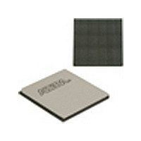
EP2SGX90EF1152I4 Altera, EP2SGX90EF1152I4 Datasheet - Page 97

EP2SGX90EF1152I4
Manufacturer Part Number
EP2SGX90EF1152I4
Description
Stratix II GX
Manufacturer
Altera
Datasheet
1.EP2SGX90EF1152I4.pdf
(316 pages)
Specifications of EP2SGX90EF1152I4
Family Name
Stratix II GX
Number Of Logic Blocks/elements
90960
# I/os (max)
558
Frequency (max)
732.1MHz
Process Technology
SRAM
Operating Supply Voltage (typ)
1.2V
Logic Cells
90960
Ram Bits
4520448
Operating Supply Voltage (min)
1.15V
Operating Supply Voltage (max)
1.25V
Operating Temp Range
-40C to 100C
Operating Temperature Classification
Industrial
Mounting
Surface Mount
Pin Count
1152
Package Type
FC-FBGA
Lead Free Status / Rohs Status
Not Compliant
Available stocks
Company
Part Number
Manufacturer
Quantity
Price
Company:
Part Number:
EP2SGX90EF1152I4
Manufacturer:
ALTERA
Quantity:
745
Company:
Part Number:
EP2SGX90EF1152I4N
Manufacturer:
ALTERA
Quantity:
535
Part Number:
EP2SGX90EF1152I4N
Manufacturer:
ALTERA/阿尔特拉
Quantity:
20 000
- Current page: 97 of 316
- Download datasheet (2Mb)
PLLs and Clock
Networks
Altera Corporation
October 2007
Stratix II GX devices provide a hierarchical clock structure and multiple
phase-locked loops (PLLs) with advanced features. The large number of
clocking resources in combination with the clock synthesis precision
provided by enhanced and fast PLLs provides a complete clock
management solution.
Global and Hierarchical Clocking
Stratix II GX devices provide 16 dedicated global clock networks and
32 regional clock networks (eight per device quadrant). These clocks are
organized into a hierarchical clock structure that allows for up to 24 clocks
per device region with low skew and delay. This hierarchical clocking
scheme provides up to 48 unique clock domains in Stratix II GX devices.
There are 12 dedicated clock pins to drive either the global or regional
clock networks. Four clock pins drive each side of the device, as shown in
Figures 2–61
can also drive the global and regional clock networks. Each global and
regional clock has a clock control block, which controls the selection of the
clock source and dynamically enables or disables the clock to reduce
power consumption.
Global Clock Network
These clocks drive throughout the entire device, feeding all device
quadrants. The global clock networks can be used as clock sources for all
resources in the device IOEs, ALMs, DSP blocks, and all memory blocks.
These resources can also be used for control signals, such as clock enables
and synchronous or asynchronous clears fed from the external pin. The
global clock networks can also be driven by internal logic for internally
Number per device
Number available per
quadrant
Sources
Dynamic clock source
selection
Dynamic enable/disable
Table 2–24. Global and Regional Clock Features
Feature
and 2–62. Internal logic and enhanced and fast PLL outputs
Table 2–24
Clock pins, PLL outputs,
inter-transceiver clocks
Global Clocks
core routings,
shows global and regional clock features.
Stratix II GX Device Handbook, Volume 1
v
v
16
16
Stratix II GX Architecture
Clock pins, PLL outputs,
inter-transceiver clocks
Regional Clocks
core routings,
v
32
—
8
2–89
Related parts for EP2SGX90EF1152I4
Image
Part Number
Description
Manufacturer
Datasheet
Request
R

Part Number:
Description:
CYCLONE II STARTER KIT EP2C20N
Manufacturer:
Altera
Datasheet:

Part Number:
Description:
CPLD, EP610 Family, ECMOS Process, 300 Gates, 16 Macro Cells, 16 Reg., 16 User I/Os, 5V Supply, 35 Speed Grade, 24DIP
Manufacturer:
Altera Corporation
Datasheet:

Part Number:
Description:
CPLD, EP610 Family, ECMOS Process, 300 Gates, 16 Macro Cells, 16 Reg., 16 User I/Os, 5V Supply, 15 Speed Grade, 24DIP
Manufacturer:
Altera Corporation
Datasheet:

Part Number:
Description:
Manufacturer:
Altera Corporation
Datasheet:

Part Number:
Description:
CPLD, EP610 Family, ECMOS Process, 300 Gates, 16 Macro Cells, 16 Reg., 16 User I/Os, 5V Supply, 30 Speed Grade, 24DIP
Manufacturer:
Altera Corporation
Datasheet:

Part Number:
Description:
High-performance, low-power erasable programmable logic devices with 8 macrocells, 10ns
Manufacturer:
Altera Corporation
Datasheet:

Part Number:
Description:
High-performance, low-power erasable programmable logic devices with 8 macrocells, 7ns
Manufacturer:
Altera Corporation
Datasheet:

Part Number:
Description:
Classic EPLD
Manufacturer:
Altera Corporation
Datasheet:

Part Number:
Description:
High-performance, low-power erasable programmable logic devices with 8 macrocells, 10ns
Manufacturer:
Altera Corporation
Datasheet:

Part Number:
Description:
Manufacturer:
Altera Corporation
Datasheet:

Part Number:
Description:
Manufacturer:
Altera Corporation
Datasheet:

Part Number:
Description:
Manufacturer:
Altera Corporation
Datasheet:

Part Number:
Description:
CPLD, EP610 Family, ECMOS Process, 300 Gates, 16 Macro Cells, 16 Reg., 16 User I/Os, 5V Supply, 25 Speed Grade, 24DIP
Manufacturer:
Altera Corporation
Datasheet:


