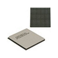
EP2SGX90EF1152I4 Altera, EP2SGX90EF1152I4 Datasheet - Page 245

EP2SGX90EF1152I4
Manufacturer Part Number
EP2SGX90EF1152I4
Description
Stratix II GX
Manufacturer
Altera
Datasheet
1.EP2SGX90EF1152I4.pdf
(316 pages)
Specifications of EP2SGX90EF1152I4
Family Name
Stratix II GX
Number Of Logic Blocks/elements
90960
# I/os (max)
558
Frequency (max)
732.1MHz
Process Technology
SRAM
Operating Supply Voltage (typ)
1.2V
Logic Cells
90960
Ram Bits
4520448
Operating Supply Voltage (min)
1.15V
Operating Supply Voltage (max)
1.25V
Operating Temp Range
-40C to 100C
Operating Temperature Classification
Industrial
Mounting
Surface Mount
Pin Count
1152
Package Type
FC-FBGA
Lead Free Status / Rohs Status
Not Compliant
Available stocks
Company
Part Number
Manufacturer
Quantity
Price
Company:
Part Number:
EP2SGX90EF1152I4
Manufacturer:
ALTERA
Quantity:
745
Company:
Part Number:
EP2SGX90EF1152I4N
Manufacturer:
ALTERA
Quantity:
535
Part Number:
EP2SGX90EF1152I4N
Manufacturer:
ALTERA/阿尔特拉
Quantity:
20 000
- Current page: 245 of 316
- Download datasheet (2Mb)
Altera Corporation
June 2009
(1)
(2)
(3)
t
t
t
t
t
t
t
t
t
t
t
t
t
t
t
MEGABESU
MEGABEH
MEGADATAASU
MEGADATAAH
MEGAADDRASU
MEGAADDRAH
MEGADATABSU
MEGADATABH
MEGAADDRBSU
MEGAADDRBH
MEGADATACO1
MEGADATACO2
MEGACLKL
MEGACLKH
MEGACLR
Table 4–61. M-RAM Block Internal Timing Microparameters (Part 2 of 2)
Symbol
The M512 block f
This column refers to –3 speed grades for EP2SGX30, EP2SGX60, and EP2SGX90 devices.
This column refers to –3 speed grades for EP2SGX130 devices.
Byte enable setup time
before clock
Byte enable hold time
after clock
A port data setup time
before clock
A port data hold time
after clock
A port address setup
time before clock
A port address hold
time after clock
B port setup time
before clock
B port hold time after
clock
B port address setup
time before clock
B port address hold
time after clock
Clock-to-output delay
when using output
registers
Clock-to-output delay
without output
registers
Minimum clock low
time
Minimum clock high
time
Minimum clear pulse
width
Parameter
MAX
obtained using the Quartus II software does not necessarily equal to 1/TMEGARC.
1950
1250
1250
Min
-347
-347
243
589
243
589
480
144
39
50
50
Grade
-9
-3 Speed
(2)
2899
Max
715
1950
1312
1312
Min
-365
-365
255
618
255
618
480
151
-10
40
52
52
Grade
-3 Speed
(3)
3042
Max
749
Stratix II GX Device Handbook, Volume 1
1950
1395
1395
Min
-388
-388
271
657
271
657
480
160
-11
DC and Switching Characteristics
43
55
55
-4 Speed
Grade
Note (1)
Max
3235
797
1950
1675
1675
-465
Min
-465
325
789
325
789
480
192
-13
-5 Speed
52
67
67
Grade
3884
Max
957
Unit
4–75
ps
ps
ps
ps
ps
ps
ps
ps
ps
ps
ps
ps
ps
ps
ps
Related parts for EP2SGX90EF1152I4
Image
Part Number
Description
Manufacturer
Datasheet
Request
R

Part Number:
Description:
CYCLONE II STARTER KIT EP2C20N
Manufacturer:
Altera
Datasheet:

Part Number:
Description:
CPLD, EP610 Family, ECMOS Process, 300 Gates, 16 Macro Cells, 16 Reg., 16 User I/Os, 5V Supply, 35 Speed Grade, 24DIP
Manufacturer:
Altera Corporation
Datasheet:

Part Number:
Description:
CPLD, EP610 Family, ECMOS Process, 300 Gates, 16 Macro Cells, 16 Reg., 16 User I/Os, 5V Supply, 15 Speed Grade, 24DIP
Manufacturer:
Altera Corporation
Datasheet:

Part Number:
Description:
Manufacturer:
Altera Corporation
Datasheet:

Part Number:
Description:
CPLD, EP610 Family, ECMOS Process, 300 Gates, 16 Macro Cells, 16 Reg., 16 User I/Os, 5V Supply, 30 Speed Grade, 24DIP
Manufacturer:
Altera Corporation
Datasheet:

Part Number:
Description:
High-performance, low-power erasable programmable logic devices with 8 macrocells, 10ns
Manufacturer:
Altera Corporation
Datasheet:

Part Number:
Description:
High-performance, low-power erasable programmable logic devices with 8 macrocells, 7ns
Manufacturer:
Altera Corporation
Datasheet:

Part Number:
Description:
Classic EPLD
Manufacturer:
Altera Corporation
Datasheet:

Part Number:
Description:
High-performance, low-power erasable programmable logic devices with 8 macrocells, 10ns
Manufacturer:
Altera Corporation
Datasheet:

Part Number:
Description:
Manufacturer:
Altera Corporation
Datasheet:

Part Number:
Description:
Manufacturer:
Altera Corporation
Datasheet:

Part Number:
Description:
Manufacturer:
Altera Corporation
Datasheet:

Part Number:
Description:
CPLD, EP610 Family, ECMOS Process, 300 Gates, 16 Macro Cells, 16 Reg., 16 User I/Os, 5V Supply, 25 Speed Grade, 24DIP
Manufacturer:
Altera Corporation
Datasheet:


