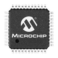
DSPIC33FJ128GP804-H/PT Microchip Technology, DSPIC33FJ128GP804-H/PT Datasheet - Page 397

DSPIC33FJ128GP804-H/PT
Manufacturer Part Number
DSPIC33FJ128GP804-H/PT
Description
16-bit DSC, 128KB Flash, CAN, DMA, 40 MIPS, NanoWatt 44 TQFP 10x10x1mm TRAY
Manufacturer
Microchip Technology
Series
dsPIC™ 33Fr
Datasheet
1.DSPIC33FJ32GP302-ISO.pdf
(412 pages)
Specifications of DSPIC33FJ128GP804-H/PT
Core Processor
dsPIC
Core Size
16-Bit
Speed
40 MIPs
Connectivity
CAN, I²C, IrDA, LIN, SPI, UART/USART
Peripherals
AC'97, Brown-out Detect/Reset, DMA, I²S, POR, PWM, WDT
Number Of I /o
35
Program Memory Size
128KB (128K x 8)
Program Memory Type
FLASH
Ram Size
16K x 8
Voltage - Supply (vcc/vdd)
3 V ~ 3.6 V
Data Converters
A/D 13x10b/12b, D/A 6x16b
Oscillator Type
Internal
Operating Temperature
-40°C ~ 140°C
Package / Case
44-TQFP
Processor Series
dsPIC33F
Core
dsPIC
Data Bus Width
16 bit
Interface Type
SPI, I2C, UART, JTAG
Number Of Programmable I/os
35
Operating Supply Voltage
3.3 V
Maximum Operating Temperature
+ 140 C
Mounting Style
SMD/SMT
Development Tools By Supplier
MPLAB IDE Software
Minimum Operating Temperature
- 40 C
On-chip Adc
10 bit, 13 Channel
A/d Bit Size
10 bit
A/d Channels Available
13
Lead Free Status / RoHS Status
Lead free / RoHS Compliant
Eeprom Size
-
Lead Free Status / Rohs Status
Details
Available stocks
Company
Part Number
Manufacturer
Quantity
Price
Company:
Part Number:
DSPIC33FJ128GP804-H/PT
Manufacturer:
Microchip Technology
Quantity:
10 000
- Current page: 397 of 412
- Download datasheet (6Mb)
TABLE A-2:
© 2011 Microchip Technology Inc.
Section 10.0 “Power-Saving
Features”
Section 11.0 “I/O Ports”
Section 16.0 “Serial Peripheral
Interface (SPI)”
Section 18.0 “Universal
Asynchronous Receiver Transmitter
(UART)”
Section 19.0 “Enhanced CAN
(ECAN™) Module”
Section 21.0 “10-Bit/12-Bit Analog-
to-Digital Converter (ADC)”
Section 22.0 “Audio Digital-to-
Analog Converter (DAC)”
Section 23.0 “Comparator Module”
Section 24.0 “Real-Time Clock and
Calendar (RTCC)”
Section 27.0 “Special Features”
dsPIC33FJ32GP302/304, dsPIC33FJ64GPX02/X04, AND dsPIC33FJ128GPX02/X04
Section Name
MAJOR SECTION UPDATES (CONTINUED)
Added the following registers:
• PMD1: Peripheral Module Disable Control Register 1 (Register 10-1)
• PMD2: Peripheral Module Disable Control Register 2 (Register 10-2)
• PMD3: Peripheral Module Disable Control Register 3 (Register 10-3)
Removed Table 11-1 and added reference to pin diagrams for I/O pin
availability and functionality.
Added paragraph on ADPCFG register default values to Section 11.3
“Configuring Analog Port Pins”.
Added Note box regarding PPS functionality with input mapping to
Section 11.6.2.1 “Input Mapping”.
Added Note 2 and 3 to the SPIxCON1 register (see Register 16-2).
Updated the Notes in the UxMode register (see Register 18-1).
Updated the UTXINV bit settings in the UxSTA register and added Note 1
(see Register 18-2).
Changed bit 11 in the ECAN Control Register 1 (CiCTRL1) to Reserved (see
Register 19-1).
Replaced the ADC1 Module Block Diagrams with new diagrams (see
Figure 21-1 and Figure 21-2).
Updated bit values for ADCS<7:0> and added Notes 1 and 2 to the ADC1
Control Register 3 (AD1CON3) (see Register 21-3).
Added Note 2 to the ADC1 Input Scan Select Register Low (AD1CSSL) (see
Register 21-7).
Added Note 2 to the ADC1 Port Configuration Register Low (AD1PCFGL)
(see Register 21-8).
Updated the midpoint voltage in the last sentence of the first paragraph.
Updated the voltage swing values in the last sentence of the last paragraph
in Section 22.3 “DAC Output Format”.
Updated the Comparator Voltage Reference Block Diagram
(see Figure 23-2).
Updated the minimum positive adjust value for CAL<7:0> in the RTCC
Calibration and Configuration (RCFGCAL) Register (see Register 24-1).
Added Note 1 to the Device Configuration Register Map (see Table 27-1).
Updated Note 1 in the dsPIC33F Configuration Bits Description (see
Table 27-2).
Update Description
DS70292E-page 397
Related parts for DSPIC33FJ128GP804-H/PT
Image
Part Number
Description
Manufacturer
Datasheet
Request
R

Part Number:
Description:
Manufacturer:
Microchip Technology Inc.
Datasheet:

Part Number:
Description:
Manufacturer:
Microchip Technology Inc.
Datasheet:

Part Number:
Description:
Manufacturer:
Microchip Technology Inc.
Datasheet:

Part Number:
Description:
Manufacturer:
Microchip Technology Inc.
Datasheet:

Part Number:
Description:
Manufacturer:
Microchip Technology Inc.
Datasheet:

Part Number:
Description:
Manufacturer:
Microchip Technology Inc.
Datasheet:

Part Number:
Description:
Manufacturer:
Microchip Technology Inc.
Datasheet:

Part Number:
Description:
Manufacturer:
Microchip Technology Inc.
Datasheet:


