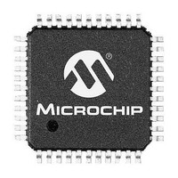
DSPIC33FJ128GP804-H/PT Microchip Technology, DSPIC33FJ128GP804-H/PT Datasheet - Page 207

DSPIC33FJ128GP804-H/PT
Manufacturer Part Number
DSPIC33FJ128GP804-H/PT
Description
16-bit DSC, 128KB Flash, CAN, DMA, 40 MIPS, NanoWatt 44 TQFP 10x10x1mm TRAY
Manufacturer
Microchip Technology
Series
dsPIC™ 33Fr
Datasheet
1.DSPIC33FJ32GP302-ISO.pdf
(412 pages)
Specifications of DSPIC33FJ128GP804-H/PT
Core Processor
dsPIC
Core Size
16-Bit
Speed
40 MIPs
Connectivity
CAN, I²C, IrDA, LIN, SPI, UART/USART
Peripherals
AC'97, Brown-out Detect/Reset, DMA, I²S, POR, PWM, WDT
Number Of I /o
35
Program Memory Size
128KB (128K x 8)
Program Memory Type
FLASH
Ram Size
16K x 8
Voltage - Supply (vcc/vdd)
3 V ~ 3.6 V
Data Converters
A/D 13x10b/12b, D/A 6x16b
Oscillator Type
Internal
Operating Temperature
-40°C ~ 140°C
Package / Case
44-TQFP
Processor Series
dsPIC33F
Core
dsPIC
Data Bus Width
16 bit
Interface Type
SPI, I2C, UART, JTAG
Number Of Programmable I/os
35
Operating Supply Voltage
3.3 V
Maximum Operating Temperature
+ 140 C
Mounting Style
SMD/SMT
Development Tools By Supplier
MPLAB IDE Software
Minimum Operating Temperature
- 40 C
On-chip Adc
10 bit, 13 Channel
A/d Bit Size
10 bit
A/d Channels Available
13
Lead Free Status / RoHS Status
Lead free / RoHS Compliant
Eeprom Size
-
Lead Free Status / Rohs Status
Details
Available stocks
Company
Part Number
Manufacturer
Quantity
Price
Company:
Part Number:
DSPIC33FJ128GP804-H/PT
Manufacturer:
Microchip Technology
Quantity:
10 000
- Current page: 207 of 412
- Download datasheet (6Mb)
17.0
The Inter-Integrated Circuit (I
complete hardware support for both Slave and Multi-
Master modes of the I
standard, with a 16-bit interface.
The I
• The SCLx pin is clock.
• The SDAx pin is data.
The I
• I
• I
• I
• I
• Serial clock synchronization for I
• I
© 2011 Microchip Technology Inc.
dsPIC33FJ32GP302/304, dsPIC33FJ64GPX02/X04, AND dsPIC33FJ128GPX02/X04
modes of operation.
addressing
addressing
master and slaves.
used as a handshake mechanism to suspend and
resume serial transfer (SCLREL control).
collision and arbitrates accordingly.
Note 1: This data sheet summarizes the features
2
2
2
2
2
C interface supporting both Master and Slave
C Slave mode supports 7-bit and 10-bit
C Master mode supports 7 and 10-bit
C Port allows bidirectional transfers between
C supports multi-master operation, detects bus
2
2
C module has a 2-pin interface:
C module offers the following key features:
2: Some registers and associated bits
INTER-INTEGRATED
CIRCUIT™ (I
of
dsPIC33FJ64GPX02/X04,
dsPIC33FJ128GPX02/X04 families of
devices. It is not intended to be a compre-
hensive reference source. To comple-
ment the information in this data sheet,
refer to “Section 19. Inter-Integrated
Circuit™ (I
“dsPIC33F/PIC24H Family Reference
Manual”, which is available from the
Microchip website (www.microchip.com).
described in this section may not be
available on all devices. Refer to
Section 4.0 “Memory Organization”
this data sheet for device-specific register
and bit information.
the
2
C™)” (DS70195) of the
2
2
dsPIC33FJ32GP302/304,
C serial communication
C™)
2
C) module provides
2
C port can be
and
in
17.1
The hardware fully implements all the master and slave
functions of the I
specifications, as well as 7 and 10-bit addressing.
The I
master on an I
The following types of I
• I
• I
• I
For details about the communication sequence in each
of these modes, refer to the “dsPIC33F/PIC24H Family
Reference Manual”. Please see the Microchip website
(www.microchip.com) for the latest dsPIC33F/PIC24H
Family Reference Manual chapters.
17.2
I2CxCON and I2CxSTAT are control and status
registers, respectively. The I2CxCON register is
readable and writable. The lower six bits of I2CxSTAT
are read-only. The remaining bits of the I2CSTAT are
read/write:
• I2CxRSR is the shift register used for shifting data
• I2CxRCV is the receive buffer and the register to
• I2CxTRN is the transmit register to which bytes
• The I2CxADD register holds the slave address.
• A status bit, ADD10, indicates 10-bit Address
• The I2CxBRG acts as the Baud Rate Generator
In receive operations, I2CxRSR and I2CxRCV together
form a double-buffered receiver. When I2CxRSR
receives a complete byte, it is transferred to I2CxRCV,
and an interrupt pulse is generated.
internal to the module and the user application
has no access to it.
which data bytes are written, or from which data
bytes are read.
are written during a transmit operation.
mode.
(BRG) reload value.
2
2
2
C slave operation with 7-bit addressing
C slave operation with 10-bit addressing
C master operation with 7-bit or 10-bit addressing
2
C module can operate either as a slave or a
Operating Modes
I
2
C Registers
2
C bus.
2
C Standard and Fast mode
2
C operation are supported:
DS70292E-page 207
Related parts for DSPIC33FJ128GP804-H/PT
Image
Part Number
Description
Manufacturer
Datasheet
Request
R

Part Number:
Description:
Manufacturer:
Microchip Technology Inc.
Datasheet:

Part Number:
Description:
Manufacturer:
Microchip Technology Inc.
Datasheet:

Part Number:
Description:
Manufacturer:
Microchip Technology Inc.
Datasheet:

Part Number:
Description:
Manufacturer:
Microchip Technology Inc.
Datasheet:

Part Number:
Description:
Manufacturer:
Microchip Technology Inc.
Datasheet:

Part Number:
Description:
Manufacturer:
Microchip Technology Inc.
Datasheet:

Part Number:
Description:
Manufacturer:
Microchip Technology Inc.
Datasheet:

Part Number:
Description:
Manufacturer:
Microchip Technology Inc.
Datasheet:


