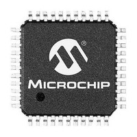
DSPIC33FJ128GP804-H/PT Microchip Technology, DSPIC33FJ128GP804-H/PT Datasheet - Page 31

DSPIC33FJ128GP804-H/PT
Manufacturer Part Number
DSPIC33FJ128GP804-H/PT
Description
16-bit DSC, 128KB Flash, CAN, DMA, 40 MIPS, NanoWatt 44 TQFP 10x10x1mm TRAY
Manufacturer
Microchip Technology
Series
dsPIC™ 33Fr
Datasheet
1.DSPIC33FJ32GP302-ISO.pdf
(412 pages)
Specifications of DSPIC33FJ128GP804-H/PT
Core Processor
dsPIC
Core Size
16-Bit
Speed
40 MIPs
Connectivity
CAN, I²C, IrDA, LIN, SPI, UART/USART
Peripherals
AC'97, Brown-out Detect/Reset, DMA, I²S, POR, PWM, WDT
Number Of I /o
35
Program Memory Size
128KB (128K x 8)
Program Memory Type
FLASH
Ram Size
16K x 8
Voltage - Supply (vcc/vdd)
3 V ~ 3.6 V
Data Converters
A/D 13x10b/12b, D/A 6x16b
Oscillator Type
Internal
Operating Temperature
-40°C ~ 140°C
Package / Case
44-TQFP
Processor Series
dsPIC33F
Core
dsPIC
Data Bus Width
16 bit
Interface Type
SPI, I2C, UART, JTAG
Number Of Programmable I/os
35
Operating Supply Voltage
3.3 V
Maximum Operating Temperature
+ 140 C
Mounting Style
SMD/SMT
Development Tools By Supplier
MPLAB IDE Software
Minimum Operating Temperature
- 40 C
On-chip Adc
10 bit, 13 Channel
A/d Bit Size
10 bit
A/d Channels Available
13
Lead Free Status / RoHS Status
Lead free / RoHS Compliant
Eeprom Size
-
Lead Free Status / Rohs Status
Details
Available stocks
Company
Part Number
Manufacturer
Quantity
Price
Company:
Part Number:
DSPIC33FJ128GP804-H/PT
Manufacturer:
Microchip Technology
Quantity:
10 000
- Current page: 31 of 412
- Download datasheet (6Mb)
3.6
The dsPIC33FJ32GP302/304, dsPIC33FJ64GPX02/
X04, and dsPIC33FJ128GPX02/X04 ALU is 16 bits
wide and is capable of addition, subtraction, bit shifts
and logic operations. Unless otherwise mentioned,
arithmetic operations are two’s complement in nature.
Depending on the operation, the ALU can affect the
values of the Carry (C), Zero (Z), Negative (N),
Overflow (OV) and Digit Carry (DC) Status bits in the
SR register. The C and DC Status bits operate as
Borrow and Digit Borrow bits, respectively, for
subtraction operations.
The ALU can perform 8-bit or 16-bit operations,
depending on the mode of the instruction that is used.
Data for the ALU operation can come from the W
register array or data memory, depending on the
addressing mode of the instruction. Likewise, output
data from the ALU can be written to the W register array
or a data memory location.
Refer to the “16-bit MCU and DSC Programmer’s Ref-
erence Manual” (DS70157) for information on the SR
bits affected by each instruction.
The dsPIC33FJ32GP302/304, dsPIC33FJ64GPX02/
X04, and dsPIC33FJ128GPX02/X04 CPU incorpo-
rates hardware support for both multiplication and divi-
sion. This includes a dedicated hardware multiplier and
support hardware for 16-bit-divisor division.
3.6.1
Using the high-speed 17-bit x 17-bit multiplier of the
DSP engine, the ALU supports unsigned, signed or
mixed-sign operation in several MCU multiplication
modes:
• 16-bit x 16-bit signed
• 16-bit x 16-bit unsigned
• 16-bit signed x 5-bit (literal) unsigned
• 16-bit unsigned x 16-bit unsigned
• 16-bit unsigned x 5-bit (literal) unsigned
• 16-bit unsigned x 16-bit signed
• 8-bit unsigned x 8-bit unsigned
3.6.2
The divide block supports 32-bit/16-bit and 16-bit/16-bit
signed and unsigned integer divide operations with the
following data sizes:
1.
2.
3.
4.
The quotient for all divide instructions ends up in W0
and the remainder in W1. 16-bit signed and unsigned
DIV instructions can specify any W register for both
the 16-bit divisor (Wn) and any W register (aligned)
pair (W(m + 1):Wm) for the 32-bit dividend. The divide
algorithm takes one cycle per bit of divisor, so both
32-bit/16-bit and 16-bit/16-bit instructions take the
same number of cycles to execute.
© 2011 Microchip Technology Inc.
dsPIC33FJ32GP302/304, dsPIC33FJ64GPX02/X04, AND dsPIC33FJ128GPX02/X04
32-bit signed/16-bit signed divide
32-bit unsigned/16-bit unsigned divide
16-bit signed/16-bit signed divide
16-bit unsigned/16-bit unsigned divide
Arithmetic Logic Unit (ALU)
MULTIPLIER
DIVIDER
3.7
The DSP engine consists of a high-speed 17-bit x
17-bit multiplier, a barrel shifter and a 40-bit adder/
subtracter (with two target accumulators, round and
saturation logic).
The dsPIC33FJ32GP302/304, dsPIC33FJ64GPX02/
X04, and dsPIC33FJ128GPX02/X04 is a single-cycle
instruction flow architecture; therefore, concurrent
operation of the DSP engine with MCU instruction flow
is not possible. However, some MCU ALU and DSP
engine resources can be used concurrently by the
same instruction (e.g., ED, EDAC).
The DSP engine can also perform inherent accumula-
tor-to-accumulator operations that require no additional
data. These instructions are ADD, SUB and NEG.
The DSP engine has options selected through bits in
the CPU Core Control register (CORCON), as listed
below:
• Fractional or integer DSP multiply (IF)
• Signed or unsigned DSP multiply (US)
• Conventional or convergent rounding (RND)
• Automatic saturation on/off for ACCA (SATA)
• Automatic saturation on/off for ACCB (SATB)
• Automatic saturation on/off for writes to data
• Accumulator Saturation mode selection
A block diagram of the DSP engine is shown in
Figure
TABLE 3-1:
CLR
ED
EDAC
MAC
MAC
MOVSAC
MPY
MPY
MPY.N
MSC
memory (SATDW)
(ACCSAT)
Instruction
3-3.
DSP Engine
DSP INSTRUCTIONS
SUMMARY
A = 0
A = (x – y)
A = A + (x – y)
A = A + (x • y)
A = A + x2
No change in A
A = x • y
A = x 2
A = – x • y
A = A – x • y
Operation
Algebraic
2
2
DS70292E-page 31
ACC Write
Back
Yes
Yes
Yes
Yes
No
No
No
No
No
No
Related parts for DSPIC33FJ128GP804-H/PT
Image
Part Number
Description
Manufacturer
Datasheet
Request
R

Part Number:
Description:
Manufacturer:
Microchip Technology Inc.
Datasheet:

Part Number:
Description:
Manufacturer:
Microchip Technology Inc.
Datasheet:

Part Number:
Description:
Manufacturer:
Microchip Technology Inc.
Datasheet:

Part Number:
Description:
Manufacturer:
Microchip Technology Inc.
Datasheet:

Part Number:
Description:
Manufacturer:
Microchip Technology Inc.
Datasheet:

Part Number:
Description:
Manufacturer:
Microchip Technology Inc.
Datasheet:

Part Number:
Description:
Manufacturer:
Microchip Technology Inc.
Datasheet:

Part Number:
Description:
Manufacturer:
Microchip Technology Inc.
Datasheet:


