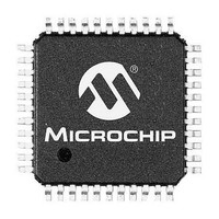
DSPIC33FJ128GP804-H/PT Microchip Technology, DSPIC33FJ128GP804-H/PT Datasheet - Page 299

DSPIC33FJ128GP804-H/PT
Manufacturer Part Number
DSPIC33FJ128GP804-H/PT
Description
16-bit DSC, 128KB Flash, CAN, DMA, 40 MIPS, NanoWatt 44 TQFP 10x10x1mm TRAY
Manufacturer
Microchip Technology
Series
dsPIC™ 33Fr
Datasheet
1.DSPIC33FJ32GP302-ISO.pdf
(412 pages)
Specifications of DSPIC33FJ128GP804-H/PT
Core Processor
dsPIC
Core Size
16-Bit
Speed
40 MIPs
Connectivity
CAN, I²C, IrDA, LIN, SPI, UART/USART
Peripherals
AC'97, Brown-out Detect/Reset, DMA, I²S, POR, PWM, WDT
Number Of I /o
35
Program Memory Size
128KB (128K x 8)
Program Memory Type
FLASH
Ram Size
16K x 8
Voltage - Supply (vcc/vdd)
3 V ~ 3.6 V
Data Converters
A/D 13x10b/12b, D/A 6x16b
Oscillator Type
Internal
Operating Temperature
-40°C ~ 140°C
Package / Case
44-TQFP
Processor Series
dsPIC33F
Core
dsPIC
Data Bus Width
16 bit
Interface Type
SPI, I2C, UART, JTAG
Number Of Programmable I/os
35
Operating Supply Voltage
3.3 V
Maximum Operating Temperature
+ 140 C
Mounting Style
SMD/SMT
Development Tools By Supplier
MPLAB IDE Software
Minimum Operating Temperature
- 40 C
On-chip Adc
10 bit, 13 Channel
A/d Bit Size
10 bit
A/d Channels Available
13
Lead Free Status / RoHS Status
Lead free / RoHS Compliant
Eeprom Size
-
Lead Free Status / Rohs Status
Details
Available stocks
Company
Part Number
Manufacturer
Quantity
Price
Company:
Part Number:
DSPIC33FJ128GP804-H/PT
Manufacturer:
Microchip Technology
Quantity:
10 000
- Current page: 299 of 412
- Download datasheet (6Mb)
27.0
dsPIC33FJ32GP302/304, dsPIC33FJ64GPX02/X04,
and
several features intended to maximize application
flexibility and reliability, and minimize cost through
elimination of external components. These are:
• Flexible configuration
• Watchdog Timer (WDT)
• Code Protection and CodeGuard™ Security
• JTAG Boundary Scan Interface
• In-Circuit Serial Programming™ (ICSP™)
• In-Circuit emulation
TABLE 27-1:
© 2011 Microchip Technology Inc.
0xF80000 FBS
0xF80002 FSS
0xF80004 FGS
0xF80006 FOSCSEL
0xF80008 FOSC
0xF8000A FWDT
0xF8000C FPOR
0xF8000E FICD
0xF80010 FUID0
0xF80012 FUID1
0xF80014 FUID2
0xF80016 FUID3
Legend: — = unimplemented bit, read as ‘0’.
Note 1:
Address
dsPIC33FJ32GP302/304, dsPIC33FJ64GPX02/X04, AND dsPIC33FJ128GPX02/X04
Note 1: This data sheet summarizes the features
dsPIC33FJ128GPX02/X04
2:
3:
2: Some registers and associated bits
SPECIAL FEATURES
This Configuration register is not available and reads as 0xFF on dsPIC33FJ32GP302/304 devices.
These bits are reserved and always read as ‘1’.
These bits are reserved for use by development tools and must be programmed as ‘1’.
of
dsPIC33FJ64GPX02/X04,
dsPIC33FJ128GPX02/X04 families of
devices. It is not intended to be a compre-
hensive reference source. To comple-
ment the information in this data sheet,
refer to the “dsPIC33F/PIC24H Family
Reference Manual”. Please see the
Microchip web site (www.microchip.com)
for the latest dsPIC33F/PIC24H Family
Reference Manual sections.
described in this section may not be avail-
able on all devices. Refer to
“Memory Organization”
sheet for device-specific register and bit
information.
Name
(1)
DEVICE CONFIGURATION REGISTER MAP
the
FWDTEN WINDIS
dsPIC33FJ32GP302/304,
IESO
Bit 7
FCKSM<1:0>
—
Reserved
RBS<1:0>
RSS<1:0>
devices
Reserved
Bit 6
in this data
(3)
Section 4.0
—
—
include
(2)
IOL1WAY
and
JTAGEN
Bit 5
—
—
—
—
—
User Unit ID Byte 0
User Unit ID Byte 1
User Unit ID Byte 2
User Unit ID Byte 3
WDTPRE
27.1
The dsPIC33FJ32GP302/304, dsPIC33FJ64GPX02/
X04, and dsPIC33FJ128GPX02/X04 devices provide
nonvolatile
configuration bits. Refer to Section 25. “Device Con-
figuration” (DS70194), in the “dsPIC33F/PIC24H
Family Reference Manual” for more information on this
implementation.
The Configuration bits can be programmed (read as
‘0’), or left unprogrammed (read as ‘1’), to select vari-
ous device configurations. These bits are mapped
starting at program memory location 0xF80000.
The individual Configuration bit descriptions for the
Configuration registers are shown in
Note that address 0xF80000 is beyond the user program
memory space. It belongs to the configuration memory
space (0x800000-0xFFFFFF), which can only be
accessed using table reads and table writes.
The Device Configuration register map is shown in
Table
ALTI2C
Bit 4
—
—
—
—
—
27-1.
Configuration Bits
—
memory
Bit 3
—
—
—
—
BSS<2:0>
SSS<2:0>
OSCIOFNC POSCMD<1:0>
WDTPOST<3:0>
implementation
Bit 2
—
GSS<1:0>
FNOSC<2:0>
FPWRT<2:0>
DS70292E-page 299
Table
Bit 1
ICS<1:0>
for
27-2.
GWRP
BWRP
SWRP
Bit 0
device
Related parts for DSPIC33FJ128GP804-H/PT
Image
Part Number
Description
Manufacturer
Datasheet
Request
R

Part Number:
Description:
Manufacturer:
Microchip Technology Inc.
Datasheet:

Part Number:
Description:
Manufacturer:
Microchip Technology Inc.
Datasheet:

Part Number:
Description:
Manufacturer:
Microchip Technology Inc.
Datasheet:

Part Number:
Description:
Manufacturer:
Microchip Technology Inc.
Datasheet:

Part Number:
Description:
Manufacturer:
Microchip Technology Inc.
Datasheet:

Part Number:
Description:
Manufacturer:
Microchip Technology Inc.
Datasheet:

Part Number:
Description:
Manufacturer:
Microchip Technology Inc.
Datasheet:

Part Number:
Description:
Manufacturer:
Microchip Technology Inc.
Datasheet:


