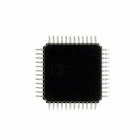
ADUC7060BSTZ32 Analog Devices Inc, ADUC7060BSTZ32 Datasheet - Page 56

ADUC7060BSTZ32
Manufacturer Part Number
ADUC7060BSTZ32
Description
DUAL 24-BIT AFE AND ARM 7 I.C
Manufacturer
Analog Devices Inc
Series
MicroConverter® ADuC7xxxr
Specifications of ADUC7060BSTZ32
Design Resources
4 mA-to-20 mA Loop-Powered Temperature Monitor Using ADuC7060/1 (CN0145) Low power, Long Range, ISM Wireless Measuring Node (CN0164)
Core Processor
ARM7
Core Size
16/32-Bit
Speed
10MHz
Connectivity
I²C, SPI, UART/USART
Peripherals
POR, PWM, Temp Sensor, WDT
Number Of I /o
14
Program Memory Size
32KB (16K x 16)
Program Memory Type
FLASH
Ram Size
4K x 8
Voltage - Supply (vcc/vdd)
2.375 V ~ 2.625 V
Data Converters
A/D 5x24b, 8x24b, D/A 1x14b
Oscillator Type
Internal
Operating Temperature
-40°C ~ 125°C
Package / Case
48-LQFP
Cpu Family
ADuC7xxx
Device Core
ARM7TDMI
Device Core Size
16/32Bit
Frequency (max)
10.24MHz
Interface Type
I2C/SPI/UART
Total Internal Ram Size
4KB
# I/os (max)
14
Number Of Timers - General Purpose
4
Operating Supply Voltage (typ)
2.5V
Operating Supply Voltage (max)
2.625V
Operating Supply Voltage (min)
2.375V
On-chip Adc
2(4-chx24-bit)
Instruction Set Architecture
RISC
Operating Temp Range
-40C to 125C
Operating Temperature Classification
Automotive
Mounting
Surface Mount
Pin Count
48
Package Type
LQFP
Package
48LQFP
Family Name
ADuC7xxx
Maximum Speed
10.24 MHz
Operating Supply Voltage
2.5 V
Data Bus Width
16|32 Bit
Number Of Programmable I/os
14
Number Of Timers
4
Lead Free Status / RoHS Status
Lead free / RoHS Compliant
Eeprom Size
-
Lead Free Status / Rohs Status
Compliant
Available stocks
Company
Part Number
Manufacturer
Quantity
Price
Company:
Part Number:
ADUC7060BSTZ32
Manufacturer:
CYPRESS
Quantity:
294
Company:
Part Number:
ADUC7060BSTZ32
Manufacturer:
ADI
Quantity:
315
Company:
Part Number:
ADUC7060BSTZ32
Manufacturer:
Analog Devices Inc
Quantity:
10 000
Part Number:
ADUC7060BSTZ32
Manufacturer:
ADI/亚德诺
Quantity:
20 000
Company:
Part Number:
ADUC7060BSTZ32-RL
Manufacturer:
Analog Devices Inc
Quantity:
10 000
ADuC7060/ADuC7061
DAC0DAT Register
Name:
Address:
Default value:
Access:
Function:
Table 64. DAC0DAT MMR Bit Designations
Bit
31:28
27:16
15:12
11:0
USING THE DAC
The on-chip DAC architecture consists of a resistor string DAC
followed by an output buffer amplifier.
The reference source for the DAC is user selectable in software. It
can be AVDD, VREF±, or ADCx/EXT_REF2IN±.
•
•
•
The DAC can be configured in three different user modes:
normal mode, DAC interpolation mode, and op amp mode.
Normal DAC Mode
In this mode of operation, the DAC is configured as a 12-bit
voltage output DAC. By default, the DAC buffer is enabled, but
the output buffer can be disabled. If the DAC output buffer is
disabled, the DAC is capable of driving a capacitive load of only
20 pF. The DAC buffer is disabled by setting the DACBUFBYPASS
bit in DAC0CON.
The DAC output buffer amplifier features a true, rail-to-rail
output stage implementation. This means that when unloaded,
each output is capable of swinging to within less than 5 mV of
both AVDD and ground. Moreover, the linearity specification of
the DAC (when driving a 5 kΩ resistive load to ground) is guar-
anteed through the full transfer function except for Code 0
to Code 100 and, in 0-to- AVDD mode only, Code 3995 to
In 0-to-AVDD mode, the DAC output transfer function
spans from 0 V to the voltage at the AVDD pin.
In VREF± and ADCx/EXT_REF2IN± modes, the DAC
output transfer function spans from negative input voltage
to the voltage positive input pin. Note that these voltages
must never go below 0 V or above AVDD.
In 0-to-V
from 0 V to the internal 1.2 V reference, V
REF
DAC0DAT
0xFFFF0604
0x00000000
Read and write
This 32-bit MMR contains the DAC output
value.
mode, the DAC output transfer function spans
Reserved.
Description
12-bit data for DAC0.
Extra four bits used in interpolation mode.
Reserved.
REF
.
Rev. B | Page 56 of 108
Code 4095. Linearity degradation near ground and AVDD is
caused by saturation of the output amplifier, and a general
representation of its effects (neglecting offset and gain error) is
illustrated in Figure 21. The dotted line in Figure 21 indicates the
ideal transfer function, and the solid line represents what the
transfer function may look like with endpoint nonlinearities due
to saturation of the output amplifier. Note that Figure 21 repre-
sents a transfer function in 0-to-AVDD mode only. In 0-to-V
or, VREF±, and ADCx/EXT_REF2IN± modes (with V
or ADCx/EXT_REF2IN± < AVDD), the lower nonlinearity is
similar. However, the upper portion of the transfer function
follows the ideal line all the way to the end (V
AVDD), showing no signs of endpoint linearity errors.
The endpoint nonlinearities conceptually illustrated in Figure 21
worsen as a function of output loading. Most of the ADuC706x
data sheet specifications in normal mode assume a 5 kΩ
resistive load to ground at the DAC output. As the output is
forced to source or sink more current, the nonlinear regions at
the top or bottom (respectively) of Figure 21 become larger.
With larger current demands, this can significantly limit output
voltage swing.
DAC Interpolation Mode
In interpolation mode, a higher DAC output resolution of 16 bits
is achieved with a longer update rate than normal mode. The
update rate is controlled by the interpolation clock rate selected
in the DAC0CON register. In this mode, an external RC filter is
required to create a constant voltage.
Op Amp Mode
In op amp mode, the DAC output buffer is used as an op amp
with the DAC itself disabled.
ADC6 is the positive input to the op amp, ADC7 is the negative
input, and ADC8 is the output. In this mode, the DAC should
be powered down by setting Bit 9 of DAC0CON.
Figure 21. Endpoint Nonlinearities Due to Amplifier Saturation
AVDD – 100mV
100mV
AVDD
0x00000000
REF
0x0FFF0000
in this case, not
REF
< AVDD
REF


