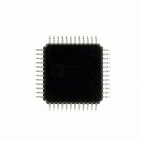
ADUC7060BSTZ32 Analog Devices Inc, ADUC7060BSTZ32 Datasheet - Page 43

ADUC7060BSTZ32
Manufacturer Part Number
ADUC7060BSTZ32
Description
DUAL 24-BIT AFE AND ARM 7 I.C
Manufacturer
Analog Devices Inc
Series
MicroConverter® ADuC7xxxr
Specifications of ADUC7060BSTZ32
Design Resources
4 mA-to-20 mA Loop-Powered Temperature Monitor Using ADuC7060/1 (CN0145) Low power, Long Range, ISM Wireless Measuring Node (CN0164)
Core Processor
ARM7
Core Size
16/32-Bit
Speed
10MHz
Connectivity
I²C, SPI, UART/USART
Peripherals
POR, PWM, Temp Sensor, WDT
Number Of I /o
14
Program Memory Size
32KB (16K x 16)
Program Memory Type
FLASH
Ram Size
4K x 8
Voltage - Supply (vcc/vdd)
2.375 V ~ 2.625 V
Data Converters
A/D 5x24b, 8x24b, D/A 1x14b
Oscillator Type
Internal
Operating Temperature
-40°C ~ 125°C
Package / Case
48-LQFP
Cpu Family
ADuC7xxx
Device Core
ARM7TDMI
Device Core Size
16/32Bit
Frequency (max)
10.24MHz
Interface Type
I2C/SPI/UART
Total Internal Ram Size
4KB
# I/os (max)
14
Number Of Timers - General Purpose
4
Operating Supply Voltage (typ)
2.5V
Operating Supply Voltage (max)
2.625V
Operating Supply Voltage (min)
2.375V
On-chip Adc
2(4-chx24-bit)
Instruction Set Architecture
RISC
Operating Temp Range
-40C to 125C
Operating Temperature Classification
Automotive
Mounting
Surface Mount
Pin Count
48
Package Type
LQFP
Package
48LQFP
Family Name
ADuC7xxx
Maximum Speed
10.24 MHz
Operating Supply Voltage
2.5 V
Data Bus Width
16|32 Bit
Number Of Programmable I/os
14
Number Of Timers
4
Lead Free Status / RoHS Status
Lead free / RoHS Compliant
Eeprom Size
-
Lead Free Status / Rohs Status
Compliant
Available stocks
Company
Part Number
Manufacturer
Quantity
Price
Company:
Part Number:
ADUC7060BSTZ32
Manufacturer:
CYPRESS
Quantity:
294
Company:
Part Number:
ADUC7060BSTZ32
Manufacturer:
ADI
Quantity:
315
Company:
Part Number:
ADUC7060BSTZ32
Manufacturer:
Analog Devices Inc
Quantity:
10 000
Part Number:
ADUC7060BSTZ32
Manufacturer:
ADI/亚德诺
Quantity:
20 000
Company:
Part Number:
ADUC7060BSTZ32-RL
Manufacturer:
Analog Devices Inc
Quantity:
10 000
Bit
4:3
2:0
Primary ADC Control Register
Name:
Address:
Default value:
Access:
Function:
Name
ADCLPMCFG[1:0]
ADCMD[2:0]
ADC0CON
0xFFFF050C
0x8000
Read and write
The primary channel ADC control MMR is a 16-bit register. If the primary ADC is reconfigured via ADC0CON, the
auxiliary ADC is also reset.
Description
ADC power mode configuration.
[00] = ADC normal mode. If enabled, the ADC operates with normal current consumption yielding optimum
electrical performance.
[01] = ADC low power mode.
[10] = ADC normal mode, same as [00].
[11] = ADC low power plus mode (low power mode and PGA off ).
ADC operation mode configuration.
[000] = ADC power-down mode. All ADC circuits and the input amplifier are powered down.
[001] = ADC continuous conversion mode. In this mode, any enabled ADC continuously converts at a
frequency equal to f
[010] = ADC single conversion mode. In this mode, any enabled ADC performs a single conversion. The ADC
enters idle mode when the single shot conversion is complete. A single conversion takes two to three ADC clock
cycles, depending on the chop mode.
[011] = ADC idle mode. In this mode, the ADC is fully powered on but is held in reset. The part enters this mode
after calibration.
[100] = ADC self-offset calibration. In this mode, an offset calibration is performed on any enabled ADC using
an internally generated 0 V. The calibration is carried out at the user-programmed ADC settings; therefore, as
with a normal single ADC conversion, it takes two to three ADC conversion cycles before a fully settled
calibration result is ready. The calibration result is automatically written to the ADCxOF MMR of the respective
ADC. The ADC returns to idle mode, and the calibration and conversion ready status bits are set at the end of
an offset calibration cycle.
Note: Always use ADC0 for single-ended self-calibration cycles on the primary ADC. Always use ADC0/ADC1
when self-calibrating for a differential input to the primary ADC.
[101] = ADC self-gain calibration. In this mode, a gain calibration against an internal reference voltage is
performed on all enabled ADCs. A gain calibration is a two-stage process and takes twice the time of an offset
calibration. The calibration result is automatically written to the ADCxGN MMR of the respective ADC. The ADC
returns to idle mode and the calibration and conversion ready status bits are set at the end of a gain calibration
cycle. An ADC self-gain calibration should only be carried out on the primary channel ADC.
Note that self-gain calibration works only when the gain = 1; do not use it when the gain > 1.
[110] = ADC system zero-scale calibration. In this mode, a zero-scale calibration is performed on enabled ADC
channels against an external zero-scale voltage driven at the ADC input pins. To do this, short the channel externally.
[111] = ADC system full-scale calibration. In this mode, a full-scale calibration is performed on enabled ADC
channels against an external full-scale voltage driven at the ADC input pins. The ADCxGN register is updated
after a full-scale calibration sequence.
ADC
. ADCxRDY must be cleared to enable new data to be written to ADC0DAT/ADC1DAT.
Rev. B | Page 43 of 108
ADuC7060/ADuC7061


