ADUC7060BSTZ32 Analog Devices Inc, ADUC7060BSTZ32 Datasheet - Page 20
ADUC7060BSTZ32
Manufacturer Part Number
ADUC7060BSTZ32
Description
DUAL 24-BIT AFE AND ARM 7 I.C
Manufacturer
Analog Devices Inc
Series
MicroConverter® ADuC7xxxr
Specifications of ADUC7060BSTZ32
Design Resources
4 mA-to-20 mA Loop-Powered Temperature Monitor Using ADuC7060/1 (CN0145) Low power, Long Range, ISM Wireless Measuring Node (CN0164)
Core Processor
ARM7
Core Size
16/32-Bit
Speed
10MHz
Connectivity
I²C, SPI, UART/USART
Peripherals
POR, PWM, Temp Sensor, WDT
Number Of I /o
14
Program Memory Size
32KB (16K x 16)
Program Memory Type
FLASH
Ram Size
4K x 8
Voltage - Supply (vcc/vdd)
2.375 V ~ 2.625 V
Data Converters
A/D 5x24b, 8x24b, D/A 1x14b
Oscillator Type
Internal
Operating Temperature
-40°C ~ 125°C
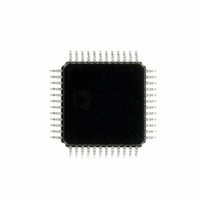
Package / Case
48-LQFP
Cpu Family
ADuC7xxx
Device Core
ARM7TDMI
Device Core Size
16/32Bit
Frequency (max)
10.24MHz
Interface Type
I2C/SPI/UART
Total Internal Ram Size
4KB
# I/os (max)
14
Number Of Timers - General Purpose
4
Operating Supply Voltage (typ)
2.5V
Operating Supply Voltage (max)
2.625V
Operating Supply Voltage (min)
2.375V
On-chip Adc
2(4-chx24-bit)
Instruction Set Architecture
RISC
Operating Temp Range
-40C to 125C
Operating Temperature Classification
Automotive
Mounting
Surface Mount
Pin Count
48
Package Type
LQFP
Package
48LQFP
Family Name
ADuC7xxx
Maximum Speed
10.24 MHz
Operating Supply Voltage
2.5 V
Data Bus Width
16|32 Bit
Number Of Programmable I/os
14
Number Of Timers
4
Lead Free Status / RoHS Status
Lead free / RoHS Compliant
Eeprom Size
-
Lead Free Status / Rohs Status
Compliant
Available stocks
Company
Part Number
Manufacturer
Quantity
Price
Company:

Part Number:
ADUC7060BSTZ32
Manufacturer:
CYPRESS
Quantity:
294
Company:
Part Number:
ADUC7060BSTZ32
Manufacturer:
ADI
Quantity:
315
Company:
Part Number:
ADUC7060BSTZ32
Manufacturer:
Analog Devices Inc
Quantity:
10 000
Part Number:
ADUC7060BSTZ32
Manufacturer:
ADI/亚德诺
Quantity:
20 000
Company:
Part Number:
ADUC7060BSTZ32-RL
Manufacturer:
Analog Devices Inc
Quantity:
10 000


ADuC7060/ADuC7061
TERMINOLOGY
Conversion Rate
The conversion rate specifies the rate at which an output result
is available from the ADC, when the ADC has settled.
The sigma-delta (Σ-Δ) conversion techniques used on this part
mean that whereas the ADC front-end signal is oversampled at
a relatively high sample rate, a subsequent digital filter is used to
decimate the output, giving a valid 24-bit data conversion result
at output rates from 1 Hz to 8 kHz.
Note that, when software switches from one input to another
(on the same ADC), the digital filter must first be cleared and
then allowed to average a new result. Depending on the con-
figuration of the ADC and the type of filter, this can take
multiple conversion cycles.
Integral Nonlinearity (INL)
INL is the maximum deviation of any code from a straight line
passing through the endpoints of the transfer function. The end-
points of the transfer function are zero scale, a point ½ LSB
below the first code transition, and full scale, a point ½ LSB
above the last code transition (111 . . . 110 to 111 . . . 111).
The error is expressed as a percentage of full scale.
No Missing Codes
No missing codes is a measure of the differential nonlinearity
of the ADC. The error is expressed in bits and specifies the
number of codes (ADC results) as 2N bits, where N is no
missing codes guaranteed to occur through the full ADC
input range.
Offset Error
Offset error is the deviation of the first code transition ADC
input voltage from the ideal first code transition.
Offset Error Drift
Offset error drift is the variation in absolute offset error with
respect to temperature. This error is expressed as least
significant bits per degree Celsius.
Gain Error
Gain error is a measure of the span error of the ADC. It is a
measure of the difference between the measured and the ideal
span between any two points in the transfer function.
Rev. B | Page 20 of 108
Output Noise
The output noise is specified as the standard deviation (or 1 ×
Sigma) of the distribution of the ADC output codes collected
when the ADC input voltage is at a dc voltage. It is expressed as
micro root mean square. The output, or root mean square (rms)
noise, can be used to calculate the effective resolution of the
ADC as defined by the following equation:
The peak-to-peak noise is defined as the deviation of codes that
fall within 6.6 × Sigma of the distribution of ADC output codes
collected when the ADC input voltage is at dc. The peak-to-peak
noise is, therefore, calculated as
The peak-to-peak noise can be used to calculate the ADC
(noise free code) resolution for which there is no code flicker
within a 6.6-Sigma limit as defined by the following equation:
Data Sheet Acronyms
ADC analog-to-digital converter
ARM advanced RISC machine
JTAG joint test action group
LSB
LVF
MCU microcontroller
MMR memory mapped register
MSB most significant byte/bit
PID
POR power-on reset
PSM power supply monitor
rms
Noise Free Code Resolution = log2
Effective Resolution = log2(Full-Scale Range/rms Noise) bits
6.6 × rms Noise
least significant byte/bit
low voltage flag
protected identifier
root mean square
⎛
⎜
⎜
⎝
Peak
Full
−
−
to
Scale
−
Peak
Range
Noise
⎞
⎟
⎟
⎠
bits
Related parts for ADUC7060BSTZ32
Image
Part Number
Description
Manufacturer
Datasheet
Request
R

Part Number:
Description:
±1.7g Dual-Axis IMEMS Accelerometer Evaluation Board
Manufacturer:
Analog Devices Inc
Datasheet:

Part Number:
Description:
Inertial Sensor Evaluation System
Manufacturer:
Analog Devices Inc
Datasheet:
Part Number:
Description:
Manufacturer:
Analog Devices Inc
Datasheet:
Part Number:
Description:
Manufacturer:
Analog Devices Inc
Datasheet:
Part Number:
Description:
Manufacturer:
Analog Devices Inc
Datasheet:
Part Number:
Description:
Manufacturer:
Analog Devices Inc
Datasheet:
Part Number:
Description:
Manufacturer:
Analog Devices Inc
Datasheet:
Part Number:
Description:
Manufacturer:
Analog Devices Inc
Datasheet:
Part Number:
Description:
Manufacturer:
Analog Devices Inc
Datasheet:
Part Number:
Description:
Manufacturer:
Analog Devices Inc
Datasheet:
Part Number:
Description:
Manufacturer:
Analog Devices Inc
Datasheet:
Part Number:
Description:
Manufacturer:
Analog Devices Inc
Datasheet:
Part Number:
Description:
Manufacturer:
Analog Devices Inc
Datasheet: