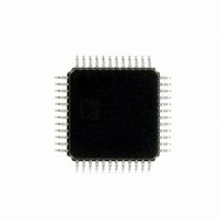
ADUC7060BSTZ32 Analog Devices Inc, ADUC7060BSTZ32 Datasheet - Page 48

ADUC7060BSTZ32
Manufacturer Part Number
ADUC7060BSTZ32
Description
DUAL 24-BIT AFE AND ARM 7 I.C
Manufacturer
Analog Devices Inc
Series
MicroConverter® ADuC7xxxr
Specifications of ADUC7060BSTZ32
Design Resources
4 mA-to-20 mA Loop-Powered Temperature Monitor Using ADuC7060/1 (CN0145) Low power, Long Range, ISM Wireless Measuring Node (CN0164)
Core Processor
ARM7
Core Size
16/32-Bit
Speed
10MHz
Connectivity
I²C, SPI, UART/USART
Peripherals
POR, PWM, Temp Sensor, WDT
Number Of I /o
14
Program Memory Size
32KB (16K x 16)
Program Memory Type
FLASH
Ram Size
4K x 8
Voltage - Supply (vcc/vdd)
2.375 V ~ 2.625 V
Data Converters
A/D 5x24b, 8x24b, D/A 1x14b
Oscillator Type
Internal
Operating Temperature
-40°C ~ 125°C
Package / Case
48-LQFP
Cpu Family
ADuC7xxx
Device Core
ARM7TDMI
Device Core Size
16/32Bit
Frequency (max)
10.24MHz
Interface Type
I2C/SPI/UART
Total Internal Ram Size
4KB
# I/os (max)
14
Number Of Timers - General Purpose
4
Operating Supply Voltage (typ)
2.5V
Operating Supply Voltage (max)
2.625V
Operating Supply Voltage (min)
2.375V
On-chip Adc
2(4-chx24-bit)
Instruction Set Architecture
RISC
Operating Temp Range
-40C to 125C
Operating Temperature Classification
Automotive
Mounting
Surface Mount
Pin Count
48
Package Type
LQFP
Package
48LQFP
Family Name
ADuC7xxx
Maximum Speed
10.24 MHz
Operating Supply Voltage
2.5 V
Data Bus Width
16|32 Bit
Number Of Programmable I/os
14
Number Of Timers
4
Lead Free Status / RoHS Status
Lead free / RoHS Compliant
Eeprom Size
-
Lead Free Status / Rohs Status
Compliant
Available stocks
Company
Part Number
Manufacturer
Quantity
Price
Company:
Part Number:
ADUC7060BSTZ32
Manufacturer:
CYPRESS
Quantity:
294
Company:
Part Number:
ADUC7060BSTZ32
Manufacturer:
ADI
Quantity:
315
Company:
Part Number:
ADUC7060BSTZ32
Manufacturer:
Analog Devices Inc
Quantity:
10 000
Part Number:
ADUC7060BSTZ32
Manufacturer:
ADI/亚德诺
Quantity:
20 000
Company:
Part Number:
ADUC7060BSTZ32-RL
Manufacturer:
Analog Devices Inc
Quantity:
10 000
ADuC7060/ADuC7061
ADC Configuration Register
Name:
Address:
Default value:
Access:
Function:
Table 48. ADCCFG MMR Bit Designations
Bit
7
6:5
4:3
2
1
0
Name
GNDSW_EN
ADC0ACCEN[1:0]
ADC0CMPEN[1:0]
ADC0OREN
GNDSW_RES_EN
ADCRCEN
ADCCFG
0xFFFF0518
0x00
Read and write
The 8-bit ADC configuration MMR controls extended functionality related to the on-chip ADCs.
Description
Analog ground switch enable.
This bit is set to 1 by user software to connect the external GND_SW pin to an internal analog ground
reference point. This bit can be used to connect and disconnect external circuits and components to ground
under program control and thereby minimize dc current consumption when the external circuit or
component is not being used. This bit is used in conjunction with ADCCFG[1] to select a 20 kΩ resistor to
ground.
When this bit is cleared, the analog ground switch is disconnected from the external pin.
Primary channel (32-bit) accumulator enable.
[00] = accumulator disabled and reset to 0. The accumulator must be disabled for a full ADC conversion
(ADCSTA[0] set twice) before the accumulator can be re-enabled to ensure that the accumulator is reset.
[01] = accumulator active. Positive current values are added to the accumulator total; the accumulator can
overflow if allowed to run for >65,535 conversions. Negative current values are subtracted from the
accumulator total; the accumulator is clamped to a minimum value of 0.
[10] = accumulator active. Same as [01] except that there is no clamp. Positive current values are added to the
accumulator total; the accumulator can overflow if allowed to run for >65,535 conversions. The absolute
values of negative current are subtracted from the accumulator total; the accumulator in this mode continues
to accumulate negatively, below 0.
[11] = accumulator and comparator active. This causes an ADC0 interrupt if ADCMSKI[6] is set.
Primary ADC comparator enable bits.
ADC0 overrange enable.
Set by the user to enable a coarse comparator on the primary channel ADC. If the reading is grossly (>30%
approximate) overrange for the active gain setting, the overrange bit in the ADCSTA MMR is set. The ADC
reading must be outside this range for greater than 125 μs for the flag to be set.
Do not use this feature in ADC low power mode.
Set to 1 to enable a 20 kΩ resistor in series with the ground switch.
Clear this bit to disable this resistor.
ADC result counter enable.
Set by user to enable the result count mode. ADC interrupts occur if ADC0RCR = ADC0RCV.
Cleared to disable the result counter. ADC interrupts occur after every conversion.
[00] = comparator disabled.
[01] = comparator active. Interrupt asserted if absolute value of ADC0 conversion result |I| ≥ ADC0TH.
[10] = comparator count mode active. Interrupt asserted if absolute value of ADC0 conversion result |I| ≥
ADC0TH for the number of ADC0THC conversions. A conversion value |I| < ADC0TH resets the threshold
counter value (ADC0THV) to 0.
[11] = comparator count mode active, interrupt asserted if absolute value of ADC0 conversion result |I| ≥
ADC0TH for the number of ADC0THC conversions. A conversion value |I| < ADC0TH decrements the threshold
counter value (ADC0THV) toward 0.
Rev. B | Page 48 of 108


