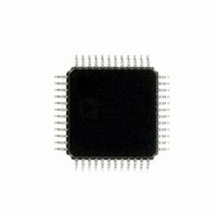
ADUC7060BSTZ32 Analog Devices Inc, ADUC7060BSTZ32 Datasheet - Page 30

ADUC7060BSTZ32
Manufacturer Part Number
ADUC7060BSTZ32
Description
DUAL 24-BIT AFE AND ARM 7 I.C
Manufacturer
Analog Devices Inc
Series
MicroConverter® ADuC7xxxr
Specifications of ADUC7060BSTZ32
Design Resources
4 mA-to-20 mA Loop-Powered Temperature Monitor Using ADuC7060/1 (CN0145) Low power, Long Range, ISM Wireless Measuring Node (CN0164)
Core Processor
ARM7
Core Size
16/32-Bit
Speed
10MHz
Connectivity
I²C, SPI, UART/USART
Peripherals
POR, PWM, Temp Sensor, WDT
Number Of I /o
14
Program Memory Size
32KB (16K x 16)
Program Memory Type
FLASH
Ram Size
4K x 8
Voltage - Supply (vcc/vdd)
2.375 V ~ 2.625 V
Data Converters
A/D 5x24b, 8x24b, D/A 1x14b
Oscillator Type
Internal
Operating Temperature
-40°C ~ 125°C
Package / Case
48-LQFP
Cpu Family
ADuC7xxx
Device Core
ARM7TDMI
Device Core Size
16/32Bit
Frequency (max)
10.24MHz
Interface Type
I2C/SPI/UART
Total Internal Ram Size
4KB
# I/os (max)
14
Number Of Timers - General Purpose
4
Operating Supply Voltage (typ)
2.5V
Operating Supply Voltage (max)
2.625V
Operating Supply Voltage (min)
2.375V
On-chip Adc
2(4-chx24-bit)
Instruction Set Architecture
RISC
Operating Temp Range
-40C to 125C
Operating Temperature Classification
Automotive
Mounting
Surface Mount
Pin Count
48
Package Type
LQFP
Package
48LQFP
Family Name
ADuC7xxx
Maximum Speed
10.24 MHz
Operating Supply Voltage
2.5 V
Data Bus Width
16|32 Bit
Number Of Programmable I/os
14
Number Of Timers
4
Lead Free Status / RoHS Status
Lead free / RoHS Compliant
Eeprom Size
-
Lead Free Status / Rohs Status
Compliant
Available stocks
Company
Part Number
Manufacturer
Quantity
Price
Company:
Part Number:
ADUC7060BSTZ32
Manufacturer:
CYPRESS
Quantity:
294
Company:
Part Number:
ADUC7060BSTZ32
Manufacturer:
ADI
Quantity:
315
Company:
Part Number:
ADUC7060BSTZ32
Manufacturer:
Analog Devices Inc
Quantity:
10 000
Part Number:
ADUC7060BSTZ32
Manufacturer:
ADI/亚德诺
Quantity:
20 000
Company:
Part Number:
ADUC7060BSTZ32-RL
Manufacturer:
Analog Devices Inc
Quantity:
10 000
ADuC7060/ADuC7061
Table 24. I
Address
0x0900
0x0904
0x0908
0x090C
0x0910
0x0914
0x0918
0x091C
0x0924
0x0928
0x092C
0x0930
0x0934
0x0938
0x093C
0x0940
0x0944
0x0948
0x094C
Table 25. SPI Base Address = 0xFFFF0A00
Address
0x0A00
0x0A04
0x0A08
0x0A0C
0x0A10
Table 26. GPIO Base Address = 0xFFFF0D00
Address
0x0D00
0x0D04
0x0D08
0x0D20
0x0D24
0x0D28
0x0D2C
0x0D30
0x0D34
0x0D38
0x0D3C
0x0D40
0x0D44
0x0D48
0x0D4C
2
Name
SPISTA
SPIRX
SPITX
SPIDIV
SPICON
Name
I2CMCON
I2CMSTA
I2CMRX
I2CMTX
I2CMCNT0
I2CMCNT1
I2CADR0
I2CADR1
I2CDIV
I2CSCON
I2CSSTA
I2CSRX
I2CSTX
I2CALT
I2CID0
I2CID1
I2CID2
I2CID3
I2CFSTA
C Base Address = 0xFFFF0900
Name
GP0CON0
GP1CON
GP2CON
GP0DAT
GP0SET
GP0CLR
GP0PAR
GP1DAT
GP1SET
GP1CLR
GP1PAR
GP2DAT
GP2SET
GP2CLR
GP2PAR
Bytes
2
2
1
1
2
1
1
1
2
2
2
1
1
1
1
1
1
1
2
Bytes
4
1
1
1
2
Bytes
4
4
4
4
4
4
4
4
4
4
4
4
4
4
4
Access Type
R/W
R
R
W
R/W
R
R/W
R/W
R/W
R/W
R/W
R
W
R/W
R/W
R/W
R/W
R/W
R/W
Access
Type
R
R
W
W
R/W
Access
Type
R/W
R/W
R/W
R/W
W
W
R/W
R/W
W
W
R/W
R/W
W
W
R/W
Default Value
0x0000
0x0000
0x00
0x00
0x0000
0x00
0x00
0x00
0x1F1F
0x0000
0x0000
0x00
0x00
0x00
0x00
0x00
0x00
0x00
0x0000
Default Value
0x00000000
0x00
0x00
0x1B
0x0000
Default Value
0x00000000
0x00000000
0x00000000
0x000000XX
0x000000XX
0x000000XX
0x00000000
0x000000XX
0x000000XX
0x000000XX
0x00000000
0x000000XX
0x000000XX
0x000000XX
0x00000000
Rev. B | Page 30 of 108
Description
I
I
I
I
I
this register prior to reading from a slave device.
I
number of bytes already received during a read from slave sequence.
Address byte register. Write the required slave address here prior to
communications.
Address byte register. Write the required slave address here prior to
communications. Only used in 10-bit mode.
I
I
I
I
I
I
I
I
I
I
I
Description
SPI status MMR.
SPI receive MMR.
SPI transmit MMR.
SPI baud rate select MMR.
SPI control MMR.
Description
GPIO Port 0 control MMR.
GPIO Port 1 control MMR.
GPIO Port 2 control MMR.
GPIO Port 0 data control MMR.
GPIO Port 0 data set MMR.
GPIO Port 0 data clear MMR.
GPIO Port 0 pull-up disable MMR.
GPIO Port 1 data control MMR.
GPIO Port 1 data set MMR.
GPIO Port 1 data clear MMR.
GPIO Port 1 pull-up disable MMR.
GPIO Port 2 data control MMR.
GPIO Port 2 data set MMR.
GPIO Port 2 data clear MMR.
GPIO Port 2 pull-up disable MMR.
2
2
2
2
2
2
2
2
2
2
2
2
2
2
2
2
2
C master control register.
C master status register.
C master receive register.
C master transmit register.
C master read count register. Write the number of required bytes into
C master current read count register. This register contains the
C clock control register. Used to configure the SCLK frequency.
C slave control register.
C slave status register.
C slave receive register.
C slave transmit register.
C hardware general call recognition register.
C Slave ID0 register. Slave bus ID register.
C Slave ID1 register. Slave bus ID register.
C Slave ID2 register. Slave bus ID register.
C Slave ID3 register. Slave bus ID register.
C FIFO status register. Used in both master and slave modes.


