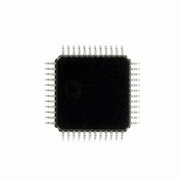
ADUC7060BSTZ32 Analog Devices Inc, ADUC7060BSTZ32 Datasheet - Page 47

ADUC7060BSTZ32
Manufacturer Part Number
ADUC7060BSTZ32
Description
DUAL 24-BIT AFE AND ARM 7 I.C
Manufacturer
Analog Devices Inc
Series
MicroConverter® ADuC7xxxr
Specifications of ADUC7060BSTZ32
Design Resources
4 mA-to-20 mA Loop-Powered Temperature Monitor Using ADuC7060/1 (CN0145) Low power, Long Range, ISM Wireless Measuring Node (CN0164)
Core Processor
ARM7
Core Size
16/32-Bit
Speed
10MHz
Connectivity
I²C, SPI, UART/USART
Peripherals
POR, PWM, Temp Sensor, WDT
Number Of I /o
14
Program Memory Size
32KB (16K x 16)
Program Memory Type
FLASH
Ram Size
4K x 8
Voltage - Supply (vcc/vdd)
2.375 V ~ 2.625 V
Data Converters
A/D 5x24b, 8x24b, D/A 1x14b
Oscillator Type
Internal
Operating Temperature
-40°C ~ 125°C
Package / Case
48-LQFP
Cpu Family
ADuC7xxx
Device Core
ARM7TDMI
Device Core Size
16/32Bit
Frequency (max)
10.24MHz
Interface Type
I2C/SPI/UART
Total Internal Ram Size
4KB
# I/os (max)
14
Number Of Timers - General Purpose
4
Operating Supply Voltage (typ)
2.5V
Operating Supply Voltage (max)
2.625V
Operating Supply Voltage (min)
2.375V
On-chip Adc
2(4-chx24-bit)
Instruction Set Architecture
RISC
Operating Temp Range
-40C to 125C
Operating Temperature Classification
Automotive
Mounting
Surface Mount
Pin Count
48
Package Type
LQFP
Package
48LQFP
Family Name
ADuC7xxx
Maximum Speed
10.24 MHz
Operating Supply Voltage
2.5 V
Data Bus Width
16|32 Bit
Number Of Programmable I/os
14
Number Of Timers
4
Lead Free Status / RoHS Status
Lead free / RoHS Compliant
Eeprom Size
-
Lead Free Status / Rohs Status
Compliant
Available stocks
Company
Part Number
Manufacturer
Quantity
Price
Company:
Part Number:
ADUC7060BSTZ32
Manufacturer:
CYPRESS
Quantity:
294
Company:
Part Number:
ADUC7060BSTZ32
Manufacturer:
ADI
Quantity:
315
Company:
Part Number:
ADUC7060BSTZ32
Manufacturer:
Analog Devices Inc
Quantity:
10 000
Part Number:
ADUC7060BSTZ32
Manufacturer:
ADI/亚德诺
Quantity:
20 000
Company:
Part Number:
ADUC7060BSTZ32-RL
Manufacturer:
Analog Devices Inc
Quantity:
10 000
Bit
7
6:0
1
2
Table 46. ADC Conversion Rates and Settling Times
Chop
Enabled
No
No
No
No
Yes
1
Table 47. Allowable Combinations of SF and AF
SF
0 to 31
32 to 63
64 to 127
Due to limitations on the digital filter internal data path, there are some limitations on the combinations of the sinc3 decimation factor (SF) and averaging factor (AF)
that can be used to generate a required ADC output rate. This restriction limits the minimum ADC update in normal power mode to 4 Hz or 1 Hz in lower power mode.
In low power mode, the ADC is driven directly by the low power oscillator (131 kHz) and not 512 kHz. All f
An additional time of approximately 60 μs per ADC is required before the first ADC is available.
Name
NOTCH2
SF[6:0]
Averaging
Factor
No
No
Yes
Yes
N/A
Description
Sinc3 modify. Set by user to modify the standard sinc3 frequency response to increase the filter stop-band rejection by
approximately 5 dB. This is achieved by inserting a second notch (NOTCH2) at
where f
Sinc3 decimation factor (SF)
sinc3 filter. The output rate from the sinc3 filter is given by
when the chop bit (Bit 15, chop enable) = 0 and the averaging factor (AF) = 0. This is valid for all SF values ≤ 125.
For SF = 126, f
For SF = 127, f
For information on calculating the f
f
f
NOTCH2
ADC
NOTCH
= (512,000/([SF + 1] × 64)) Hz
Running
Average
No
Yes
No
Yes
N/A
= 1.333 × f
is the location of the first notch in the response.
0
Yes
Yes
Yes
ADC
ADC
is forced to 60 Hz.
is forced to 50 Hz.
NOTCH
f
[
[
[
[
[
ADC
SF
SF
SF
SF
SF
512
512
Normal Mode
+
+
+
+
+
1
] 1
] 1
] 1
,
] 1
,
] 1
.The value (SF) written in these bits controls the oversampling (decimation factor) of the
000
000
512
512
×
×
×
×
×
512
64
64
64
64
64
1 to 7
Yes
Yes
No
,
,
000
000
×
×
×
,
000
ADC
3 [
3 [ AF
3 [ AF
2
+
+
+
for SF (other than 126 and 127) and AF values, refer to Table 46.
AF
Rev. B | Page 47 of 108
]
]
]
+
3
8 to 63
Yes
No
No
f
[
[
[
[
[
ADC
SF
SF
SF
SF
SF
131
131
+
Low Power Mode
+
+
+
+
] 1
] 1
] 1
,
,
] 1
] 1
072
072
131
131
×
×
×
×
×
131
64
64
64
,
64
64
,
072
AF Range
072
×
×
×
,
072
3 [
[
3 [
3 AF
+
+
+
AF
AF
ADC
]
]
]
+
calculations should be divided by 4 (approximately).
3
t
SETTLING
f
f
f
f
f
ADC
ADC
ADC
ADC
ADC
3
4
1
2
2
ADuC7060/ADuC7061
1


