ADSP-2189MBSTZ-266 Analog Devices Inc, ADSP-2189MBSTZ-266 Datasheet - Page 9
ADSP-2189MBSTZ-266
Manufacturer Part Number
ADSP-2189MBSTZ-266
Description
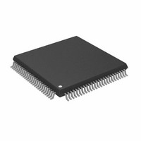
IC,DSP,16-BIT,CMOS,QFP,100PIN,PLASTIC
Manufacturer
Analog Devices Inc
Series
ADSP-21xxr
Type
Fixed Pointr
Datasheet
1.ADSP-2189MBSTZ-266.pdf
(32 pages)
Specifications of ADSP-2189MBSTZ-266
Interface
Host Interface, Serial Port
Clock Rate
66MHz
Non-volatile Memory
External
On-chip Ram
192kB
Voltage - I/o
3.30V
Voltage - Core
2.50V
Operating Temperature
-40°C ~ 85°C
Mounting Type
Surface Mount
Package / Case
100-LQFP
Device Core Size
16b
Format
Fixed Point
Clock Freq (max)
66MHz
Mips
66
Device Input Clock Speed
66MHz
Ram Size
192KB
Operating Supply Voltage (typ)
2.5/3.3V
Operating Supply Voltage (min)
2.25V
Operating Supply Voltage (max)
2.75/3.6V
Operating Temp Range
-40C to 85C
Operating Temperature Classification
Industrial
Mounting
Surface Mount
Pin Count
100
Package Type
LQFP
Lead Free Status / RoHS Status
Lead free / RoHS Compliant
Lead Free Status / RoHS Status
Lead free / RoHS Compliant
Other names
ADSP-2189MBSTZ266
Available stocks
Company
Part Number
Manufacturer
Quantity
Price
Company:

Part Number:
ADSP-2189MBSTZ-266
Manufacturer:
MICROCHIP
Quantity:
16 700
Company:
Part Number:
ADSP-2189MBSTZ-266
Manufacturer:
AD
Quantity:
5 510
Company:
Part Number:
ADSP-2189MBSTZ-266
Manufacturer:
Analog Devices Inc
Quantity:
10 000


Data Memory, Host Mode allows access to all internal
memory. External overlay access is limited by a single external
address line (A0).
PMOVLAY
Memory Mapped Registers (New to the ADSP-2189M)
The ADSP-2189M has three memory mapped registers that
differ from other ADSP-21xx Family DSPs. The slight modifi-
cations to these registers (Wait-State Control, Programmable
Flag and Composite Select Control and System Control) pro-
vide the ADSP-2189M’s wait-state and BMS control features.
Figure 7. Programmable Flag and Composite Select Con-
trol Register
REV. A
WAIT STATE MODE SELECT (ADSP-2189M)
0 = NORMAL MODE (DWAIT, IOWAIT0-3 = N WAIT STATES, RANGING FROM 0 TO 7)
1 = 2N+1 MODE (DWAIT, IOWAIT0-3 = N WAIT STATES, RANGING FROM 0 TO 15)
0, 4, 5, 6, 7
1
2
SPORT0 ENABLE
0 = DISABLE
1 = ENABLE
(BIT-15, ADSP-2189M)
SPORT1 CONFIGURE
0 = FI, FO, IRQ0, IRQ1, SCLK
1 = SPORT1
15 14 13 12 11 10 9
Figure 6. Wait-State Control Register (ADSP-2189M)
0
15 14 13 12 11 10 9
SPORT1 ENABLE
0 = DISABLE
1 = ENABLE
1
15 14 13 12 11 10 9
1
PROGRAMMABLE FLAG & COMPOSITE SELECT CONTROL
0
BMWAIT
1
DWAIT
1
0
1
1
0
1
Figure 8. System Control Register
1
Memory
Internal
External
Overlay 1
External
Overlay 2
(WHERE BIT: 11-IOM, 10BM, 9-DM, 8-PM)
0
1
IOWAIT3
1
WAIT-STATE CONTROL
1
Table IV. DMOVLAY Bits
1
SYSTEM CONTROL
RESERVED, ALWAYS = 0
CMSSEL
0 = DISABLE CMS
1 = ENABLE CMS
1
0
1
1
8
(ADSP-2189M)
0
8
1
IOWAIT2
8
1
7
0
A13
Not Applicable Not Applicable
0
1
7
1
7
1
DISABLE BMS (ADSP-2189M)
0 = ENABLE BMS
1 = DISABLE BMS, EXCEPT WHEN MEMORY
6
0
6
1
STROBES ARE THREE-STATED
6
1
5
0
5
1
IOWAIT1
5
1
4
0
4
1
PFTYPE
0 = INPUT
1 = OUTPUT
4
1
3
0
3
1
3
1
PWAIT
PROGRAM MEMORY
WAIT STATES
2
1
2
1
IOWAIT0
2
1
1
1
A12:0
13 LSBs of Address
Between 0x2000
and 0x3FFF
13 LSBs of Address
Between 0x2000
and 0x3FFF
1
1
1
1
0
1
0
1
0
1
DM(0x3FFF)
DM(0x3FFE)
DM(0x3FE6)
–9–
I/O Space (Full Memory Mode)
The ADSP-2189M supports an additional external memory
space called I/O space. This space is designed to support simple
connections to peripherals (such as data converters and external
registers) or to bus interface ASIC data registers. I/O space
supports 2048 locations of 16-bit-wide data. The lower eleven
bits of the external address bus are used; the upper three bits are
undefined. Two instructions were added to the core ADSP-2100
Family instruction set to read from and write to I/O memory
space. The I/O space also has four dedicated three-bit wait-state
registers, IOWAIT0–3, which, in combination with the wait-
state mode bit, specify up to 15 wait-states to be automatically
generated for each of four regions. The wait-states act on ad-
dress ranges as shown in Table V.
Address Range
0x000–0x1FF
0x200–0x3FF
0x400–0x5FF
0x600–0x7FF
Composite Memory Select (CMS)
The ADSP-2189M has a programmable memory select signal
that is useful for generating memory select signals for memories
mapped to more than one space. The CMS signal is generated
to have the same timing as each of the individual memory
select signals (PMS, DMS, BMS, IOMS) but can combine
their functionality.
When set, each bit in the CMSSEL register causes the CMS
signal to be asserted when the selected memory select is as-
serted. For example, to use a 32K word memory to act as both
program and data memory, set the PMS and DMS bits in the
CMSSEL register and use the CMS pin to drive the chip select
of the memory, and use either DMS or PMS as the additional
address bit.
The CMS pin functions like the other memory select signals,
with the same timing and bus request logic. A 1 in the enable bit
causes the assertion of the CMS signal at the same time as the
selected memory select signal. All enable bits default to 1 at
reset, except the BMS bit.
Byte Memory Select (BMS)
The ADSP-2189M’s BMS disable feature combined with the
CMS pin lets you use multiple memories in the byte memory
space. For example, an EPROM could be attached to the BMS
select, and an SRAM could be connected to CMS. Because
BMS is enabled at reset, the EPROM would be used for boot-
ing. After booting, software could disable BMS and set the
CMS signal to respond to BMS, enabling the SRAM.
Wait-State Register
IOWAIT0 and Wait-State Mode Select Bit
IOWAIT1 and Wait-State Mode Select Bit
IOWAIT2 and Wait-State Mode Select Bit
IOWAIT3 and Wait-State Mode Select Bit
Table V. Wait-States
ADSP-2189M
Related parts for ADSP-2189MBSTZ-266
Image
Part Number
Description
Manufacturer
Datasheet
Request
R

Part Number:
Description:
±1.7g Dual-Axis IMEMS Accelerometer Evaluation Board
Manufacturer:
Analog Devices Inc
Datasheet:

Part Number:
Description:
Inertial Sensor Evaluation System
Manufacturer:
Analog Devices Inc
Datasheet:
Part Number:
Description:
Manufacturer:
Analog Devices Inc
Datasheet:
Part Number:
Description:
Manufacturer:
Analog Devices Inc
Datasheet:
Part Number:
Description:
Manufacturer:
Analog Devices Inc
Datasheet:
Part Number:
Description:
Manufacturer:
Analog Devices Inc
Datasheet:
Part Number:
Description:
Manufacturer:
Analog Devices Inc
Datasheet:
Part Number:
Description:
Manufacturer:
Analog Devices Inc
Datasheet:
Part Number:
Description:
Manufacturer:
Analog Devices Inc
Datasheet:
Part Number:
Description:
Manufacturer:
Analog Devices Inc
Datasheet:
Part Number:
Description:
Manufacturer:
Analog Devices Inc
Datasheet:
Part Number:
Description:
Manufacturer:
Analog Devices Inc
Datasheet:
Part Number:
Description:
Manufacturer:
Analog Devices Inc
Datasheet: