ADSP-2189MBSTZ-266 Analog Devices Inc, ADSP-2189MBSTZ-266 Datasheet - Page 16
ADSP-2189MBSTZ-266
Manufacturer Part Number
ADSP-2189MBSTZ-266
Description
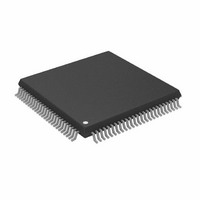
IC,DSP,16-BIT,CMOS,QFP,100PIN,PLASTIC
Manufacturer
Analog Devices Inc
Series
ADSP-21xxr
Type
Fixed Pointr
Datasheet
1.ADSP-2189MBSTZ-266.pdf
(32 pages)
Specifications of ADSP-2189MBSTZ-266
Interface
Host Interface, Serial Port
Clock Rate
66MHz
Non-volatile Memory
External
On-chip Ram
192kB
Voltage - I/o
3.30V
Voltage - Core
2.50V
Operating Temperature
-40°C ~ 85°C
Mounting Type
Surface Mount
Package / Case
100-LQFP
Device Core Size
16b
Format
Fixed Point
Clock Freq (max)
66MHz
Mips
66
Device Input Clock Speed
66MHz
Ram Size
192KB
Operating Supply Voltage (typ)
2.5/3.3V
Operating Supply Voltage (min)
2.25V
Operating Supply Voltage (max)
2.75/3.6V
Operating Temp Range
-40C to 85C
Operating Temperature Classification
Industrial
Mounting
Surface Mount
Pin Count
100
Package Type
LQFP
Lead Free Status / RoHS Status
Lead free / RoHS Compliant
Lead Free Status / RoHS Status
Lead free / RoHS Compliant
Other names
ADSP-2189MBSTZ266
Available stocks
Company
Part Number
Manufacturer
Quantity
Price
Company:

Part Number:
ADSP-2189MBSTZ-266
Manufacturer:
MICROCHIP
Quantity:
16 700
Company:
Part Number:
ADSP-2189MBSTZ-266
Manufacturer:
AD
Quantity:
5 510
Company:
Part Number:
ADSP-2189MBSTZ-266
Manufacturer:
Analog Devices Inc
Quantity:
10 000


ADSP-2189M
FREQUENCY DEPENDENCY FOR TIMING
SPECIFICATIONS
t
with a frequency equal to half the instruction rate: a 37.50 MHz
input clock (which is equivalent to 28 ns) yields a 13 ns proces-
sor cycle (equivalent to 75 MHz). t
0.5t
rameters to obtain the specification value.
Example: t
ENVIRONMENTAL CONDITIONS
Rating Description
Thermal Resistance
NOTE
1
POWER DISSIPATION
To determine total power dissipation in a specific application,
the following equation should be applied for each output:
C = load capacitance, f = output switching frequency.
Example:
In an application where external data memory is used and no
other outputs are active, power dissipation is calculated as follows:
Assumptions:
• External data memory is accessed every cycle with 50% of
• External data memory writes occur every other cycle with
• Each address and data pin has a 10 pF total load at the pin.
• The application operates at V
P
graph (Figure 15).
(C × V
Parameters
Address, DMS
Data Output, WR 9
RD
CLKOUT
Total power dissipation for this example is P
Where the ambient temperature rating (T
CK
INT
T
T
PD = Power dissipation in W.
(Case-to-Ambient)
(Junction-to-Ambient)
(Junction-to-Case)
AMB
CASE
the address pins switching.
50% of the data pins switching.
is defined as 0.5t
CKI
= internal power dissipation from Power vs. Frequency
= T
DDEXT
= Case temperature in °C
period should be substituted for all relevant timing pa-
Total Power Dissipation = P
CASE
CKH
2
– (PD × θ
× f) is calculated for each output:
= 0.5t
# of
Pins C
8
1
1
CKI
CA
CK
)
. The ADSP-2189M uses an input clock
10 pF 3.3
10 pF 3.3
10 pF 3.3
10 pF 3.3
– 7 ns = 0.5 (15 ns) – 7 ns = 0.5 ns
C × V
DD
V
DDEXT
DDEXT
AMB
INT
2
CK
2
2
2
2
× f
V
V
V
V
) is:
1
+ (C × V
values within the range of
= 3.3 V and t
Symbol
θ
θ
θ
2
CA
JA
JC
f
33.3 MHz
16.67 MHz 16.3 mW
16.67 MHz
33.3 MHz
INT
DDEXT
+ 50.7 mW.
2
CK
× f)
Value
48°C/W
50°C/W
2°C/W
PD
29.0 mW
50.7 mW
= 15 ns.
1.8 mW
3.6 mW
–16–
Output Drive Currents
Figure 14 shows typical I-V characteristics for the output drivers
on the ADSP-2189M. The curves represent the current drive
capability of the output drivers as a function of output voltage.
Figure 14. Typical Output Driver Characteristics
–20
–40
–60
–80
80
60
40
20
0
0
V
V
V
0.5
DDEXT
DDEXT
DDEXT
= 3.3V @ +25 C
= 3.6V @ –40 C
= 2.5V @ +85 C
1.0
V
OL
SOURCE VOLTAGE – V
1.5
V
DDEXT
2.0
V
DDEXT
V
= 3.6V @ –40 C
OH
V
2.5
DDEXT
= 2.5V @ +85 C
= 3.3V @ +25 C
3.0
3.5
4.0
REV. A
Related parts for ADSP-2189MBSTZ-266
Image
Part Number
Description
Manufacturer
Datasheet
Request
R

Part Number:
Description:
±1.7g Dual-Axis IMEMS Accelerometer Evaluation Board
Manufacturer:
Analog Devices Inc
Datasheet:

Part Number:
Description:
Inertial Sensor Evaluation System
Manufacturer:
Analog Devices Inc
Datasheet:
Part Number:
Description:
Manufacturer:
Analog Devices Inc
Datasheet:
Part Number:
Description:
Manufacturer:
Analog Devices Inc
Datasheet:
Part Number:
Description:
Manufacturer:
Analog Devices Inc
Datasheet:
Part Number:
Description:
Manufacturer:
Analog Devices Inc
Datasheet:
Part Number:
Description:
Manufacturer:
Analog Devices Inc
Datasheet:
Part Number:
Description:
Manufacturer:
Analog Devices Inc
Datasheet:
Part Number:
Description:
Manufacturer:
Analog Devices Inc
Datasheet:
Part Number:
Description:
Manufacturer:
Analog Devices Inc
Datasheet:
Part Number:
Description:
Manufacturer:
Analog Devices Inc
Datasheet:
Part Number:
Description:
Manufacturer:
Analog Devices Inc
Datasheet:
Part Number:
Description:
Manufacturer:
Analog Devices Inc
Datasheet: