ADSP-2189MBSTZ-266 Analog Devices Inc, ADSP-2189MBSTZ-266 Datasheet - Page 14
ADSP-2189MBSTZ-266
Manufacturer Part Number
ADSP-2189MBSTZ-266
Description
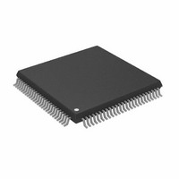
IC,DSP,16-BIT,CMOS,QFP,100PIN,PLASTIC
Manufacturer
Analog Devices Inc
Series
ADSP-21xxr
Type
Fixed Pointr
Datasheet
1.ADSP-2189MBSTZ-266.pdf
(32 pages)
Specifications of ADSP-2189MBSTZ-266
Interface
Host Interface, Serial Port
Clock Rate
66MHz
Non-volatile Memory
External
On-chip Ram
192kB
Voltage - I/o
3.30V
Voltage - Core
2.50V
Operating Temperature
-40°C ~ 85°C
Mounting Type
Surface Mount
Package / Case
100-LQFP
Device Core Size
16b
Format
Fixed Point
Clock Freq (max)
66MHz
Mips
66
Device Input Clock Speed
66MHz
Ram Size
192KB
Operating Supply Voltage (typ)
2.5/3.3V
Operating Supply Voltage (min)
2.25V
Operating Supply Voltage (max)
2.75/3.6V
Operating Temp Range
-40C to 85C
Operating Temperature Classification
Industrial
Mounting
Surface Mount
Pin Count
100
Package Type
LQFP
Lead Free Status / RoHS Status
Lead free / RoHS Compliant
Lead Free Status / RoHS Status
Lead free / RoHS Compliant
Other names
ADSP-2189MBSTZ266
Available stocks
Company
Part Number
Manufacturer
Quantity
Price
Company:

Part Number:
ADSP-2189MBSTZ-266
Manufacturer:
MICROCHIP
Quantity:
16 700
Company:
Part Number:
ADSP-2189MBSTZ-266
Manufacturer:
AD
Quantity:
5 510
Company:
Part Number:
ADSP-2189MBSTZ-266
Manufacturer:
Analog Devices Inc
Quantity:
10 000


RECOMMENDED OPERATING CONDITIONS
Parameter
V
V
V
T
NOTES
1
ELECTRICAL CHARACTERISTICS
Parameter
V
V
V
V
V
I
I
I
I
I
I
I
I
I
C
C
NOTES
10
11
12
13
14
15
Specifications subject to change without notice.
ADSP-2189M–SPECIFICATIONS
1
5
The ADSP-2189M is 3.3 V tolerant (always accepts up to 3.6 Volt max V
(max) ≈ V
RESET, BR, DR0, DR1, PWD).
IH
IL
OZH
OZL
DD
DD
DD
DD
DD
2
3
4
6
7
8
9
Bidirectional pins: D0–D23, RFS0, RFS1, SCLK0, SCLK1, TFS0, TFS1, A1–A13, PF0–PF7.
Although specified for TTL outputs, all ADSP-2189M outputs are CMOS-compatible and will drive to V
DDINT
DDEXT
INPUT
IH
IH
IL
OH
OL
Input Only pins: RESET, BR, DR0, DR1, PWD.
Input Only pins: CLKIN, RESET, BR, DR0, DR1, PWD.
Output pins: BG, PMS, DMS, BMS, IOMS, CMS, RD, WR, PWDACK, A0, DT0, DT1, CLKOUT, FL2-0, BGH.
Guaranteed but not tested.
Three-statable pins: A0–A13, D0-D23, PMS, DMS, BMS, IOMS, CMS, RD, WR, DT0, DT1, SCLK0, SCLK1, TFS0, TFS1, RFS0, RFS1, PF0–PF7.
0 V on BR.
Idle refers to ADSP-2189M state of operation during execution of IDLE instruction. Deasserted pins are driven to either V
I
and type 6, and 20% are idle instructions.
V
See Chapter 9 of the ADSP-2100 Family User’s Manual, Third Edition for details.
Applies to LQFP package type.
Output pin capacitance is the capacitive load for any three-stated output pin.
V
AMB
I
O
DD
, Input Pin Capacitance
, Lo-Level Input Current
, Hi-Level Input Current
IN
DDINT
, Output Pin Capacitance
, Lo-Level Input Voltage
, Supply Current (Idle)
, Supply Current (Idle)
, Supply Current (Dynamic)
, Supply Current (Dynamic)
, Supply Current (Power-Down)
, Hi-Level Input Voltage
, Hi-Level CLKIN Voltage
, Lo-Level Output Voltage
, Hi-Level Output Voltage
, Three-State Leakage Current
, Three-State Leakage Current
measurement taken with all instructions executing from internal memory. 50% of the instructions are multifunction (types 1, 4, 5, 12, 13, 14), 30% are type 2
= 0 V and 3 V. For typical figures for supply currents, refer to Power Dissipation section.
1
= 2.5 V. T = 25°C.
DDEXT
(max). This applies to Bidirectional pins (D0–D23, RFS0, RFS1, SCLK0, SCLK1, TFS0, TFS1, A1–A13, PF0–PF7) and Input Only pins (CLKIN,
3, 6, 13
9
9
3
3
1, 2
1, 3
6, 7, 12, 14
1, 4, 5
1, 4 , 5
10
10
7
7
12, 15
Test Conditions
@ V
@ V
@ V
@ V
@ V
@ V
@ V
@ V
@ V
@ V
@ V
@ V
@ V
@ V
@ V
Lowest Power Mode
@ V
@ V
T
T
f
T
f
T
IN
IN
DDINT
DDINT
DDINT
DDEXT
DDEXT
DDEXT
DDEXT
DDINT
DDINT
DDINT
DDINT
DDINT
DDINT
DDINT
DDINT
IN
IN
AMB
AMB
AMB
AMB
= 1.0 MHz,
= 1.0 MHz,
= 2.5 V,
= 2.5 V,
= +25°C
= +25°C
= +25°C
= +25°C
= max
= max
= min
= max, V
= max, V
= max, V
= max, V
= 2.5, t
= 2.5, t
= 2.5, t
= 2.5, t
= min, I
= 3.0 V, I
= min, I
= min, I
IH)
, but voltage compliance (on outputs, V
CK
CK
CK
CK
OH
OH
–14–
Min
2.37
2.37
V
0
OL
IN
IN
IN
IN
OH
IL
= 15 ns
= 13.3 ns
= 15 ns
= 13.3 ns
= –0.5 mA
= –100 µA
= 3.6 V
= 0 V
= 3.6 V
= 0 V
= 2 mA
= –0.3
= –0.5 mA
K Grade
8
11
8
,
11
,
6
Max
2.63
3.6
V
+70
IH
= 3.6
Min
1.5
2.0
2.0
2.4
V
DDEXT
DDEXT
and GND, assuming no dc loads.
– 0.3
OH
) depends on the input V
K/B Grades
Min
2.25
2.25
–0.03
–40
Typ
9
10
32
36
150
DD
or GND.
B Grade
Max
2.75
3.6
3.6
+85
Max
0.6
0.4
10
10
10
10
8
8
DDEXT
; because V
REV. A
Unit
V
V
V
°C
Unit
V
V
V
V
V
V
V
µA
µA
µA
µA
mA
mA
mA
mA
µA
pF
pF
OH
Related parts for ADSP-2189MBSTZ-266
Image
Part Number
Description
Manufacturer
Datasheet
Request
R

Part Number:
Description:
±1.7g Dual-Axis IMEMS Accelerometer Evaluation Board
Manufacturer:
Analog Devices Inc
Datasheet:

Part Number:
Description:
Inertial Sensor Evaluation System
Manufacturer:
Analog Devices Inc
Datasheet:
Part Number:
Description:
Manufacturer:
Analog Devices Inc
Datasheet:
Part Number:
Description:
Manufacturer:
Analog Devices Inc
Datasheet:
Part Number:
Description:
Manufacturer:
Analog Devices Inc
Datasheet:
Part Number:
Description:
Manufacturer:
Analog Devices Inc
Datasheet:
Part Number:
Description:
Manufacturer:
Analog Devices Inc
Datasheet:
Part Number:
Description:
Manufacturer:
Analog Devices Inc
Datasheet:
Part Number:
Description:
Manufacturer:
Analog Devices Inc
Datasheet:
Part Number:
Description:
Manufacturer:
Analog Devices Inc
Datasheet:
Part Number:
Description:
Manufacturer:
Analog Devices Inc
Datasheet:
Part Number:
Description:
Manufacturer:
Analog Devices Inc
Datasheet:
Part Number:
Description:
Manufacturer:
Analog Devices Inc
Datasheet: