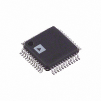
AD9753ASTZ Analog Devices Inc, AD9753ASTZ Datasheet - Page 6

AD9753ASTZ
Manufacturer Part Number
AD9753ASTZ
Description
12-Bit, 300 MSPS TxDAC+ DAC
Manufacturer
Analog Devices Inc
Series
TxDAC+®r
Datasheet
1.AD9753ASTZ.pdf
(28 pages)
Specifications of AD9753ASTZ
Settling Time
11ns
Number Of Bits
12
Data Interface
Parallel
Number Of Converters
1
Voltage Supply Source
Analog and Digital
Power Dissipation (max)
165mW
Operating Temperature
-40°C ~ 85°C
Mounting Type
Surface Mount
Package / Case
48-LQFP
Number Of Channels
1
Resolution
12b
Interface Type
Parallel
Single Supply Voltage (typ)
3.3V
Dual Supply Voltage (typ)
Not RequiredV
Architecture
Segment
Power Supply Requirement
Analog and Digital
Output Type
Current
Single Supply Voltage (min)
3V
Single Supply Voltage (max)
3.6V
Dual Supply Voltage (min)
Not RequiredV
Dual Supply Voltage (max)
Not RequiredV
Operating Temp Range
-40C to 85C
Operating Temperature Classification
Industrial
Mounting
Surface Mount
Pin Count
48
Package
48LQFP
Conversion Rate
300 MSPS
Digital Interface Type
Parallel
Number Of Outputs Per Chip
1
Full Scale Error
±2 %FSR
Integral Nonlinearity Error
±1.5 LSB
Maximum Settling Time
0.011(Typ) us
Lead Free Status / RoHS Status
Lead free / RoHS Compliant
For Use With
AD9753-EB - BOARD EVAL FOR AD9753
Lead Free Status / Rohs Status
Compliant
Available stocks
Company
Part Number
Manufacturer
Quantity
Price
Company:
Part Number:
AD9753ASTZ
Manufacturer:
Analog Devices Inc
Quantity:
10 000
Part Number:
AD9753ASTZ
Manufacturer:
ADI/亚德诺
Quantity:
20 000
Company:
Part Number:
AD9753ASTZRL
Manufacturer:
Analog Devices Inc
Quantity:
10 000
AD9753
Pin No.
1
2
3
4, 22
5, 21
6
7–18
19–20, 35–36
23–34
37, 38
39
40
41
42
43
44
45
46
47
48
Mnemonic
RESET
CLK+
CLK–
DCOM
DVDD
PLLLOCK
P1B11–P1B0
RESERVED
P2B11–P2B0
DIV0, DIV1
REFIO
FSADJ
AVDD
I
I
ACOM
CLKCOM
LPF
PLLVDD
CLKVDD
OUTB
OUTA
MSB–P1B11
PLLLOCK
RESET
DCOM
P1B10
DVDD
CLK+
CLK–
P1B9
P1B8
P1B7
P1B6
Description
Internal Clock Divider Reset
Differential Clock Input
Differential Clock Input
Digital Common
Digital Supply Voltage
Phase-Locked Loop Lock Indicator Output
Data Bits DB11 to DB0, Port 1
Data Bits DB11 to DB0, Port 2
Control Inputs for PLL and Input Port Selector Mode. See Tables I and II for details.
Reference Input/Output
Full-Scale Current Output Adjust
Analog Supply Voltage
Differential DAC Current Output
Differential DAC Current Output
Analog Common
Clock and Phase-Locked Loop Common
Phase-Locked Loop Filter
Phase-Locked Loop Supply Voltage
Clock Supply Voltage
10
11
12
1
2
3
4
5
6
7
8
9
PIN FUNCTION DESCRIPTIONS
48 47 46 45 44
13 14 15 16 17 18 19 20 21 22 23 24
PIN 1
IDENTIFIER
PIN CONFIGURATION
(Not to Scale)
AD9753
TOP VIEW
43 42 41 40
–6–
39 38 37
RESERVED = NO
USER CONNECTIONS
36
35
34
33
32
31
30
29
28
27
26
25
RESERVED
RESERVED
P2B0–LSB
P2B1
P2B2
P2B3
P2B4
P2B5
P2B6
P2B7
P2B8
P2B9
REV. B


