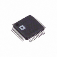
AD9753ASTZ Analog Devices Inc, AD9753ASTZ Datasheet - Page 12

AD9753ASTZ
Manufacturer Part Number
AD9753ASTZ
Description
12-Bit, 300 MSPS TxDAC+ DAC
Manufacturer
Analog Devices Inc
Series
TxDAC+®r
Datasheet
1.AD9753ASTZ.pdf
(28 pages)
Specifications of AD9753ASTZ
Settling Time
11ns
Number Of Bits
12
Data Interface
Parallel
Number Of Converters
1
Voltage Supply Source
Analog and Digital
Power Dissipation (max)
165mW
Operating Temperature
-40°C ~ 85°C
Mounting Type
Surface Mount
Package / Case
48-LQFP
Number Of Channels
1
Resolution
12b
Interface Type
Parallel
Single Supply Voltage (typ)
3.3V
Dual Supply Voltage (typ)
Not RequiredV
Architecture
Segment
Power Supply Requirement
Analog and Digital
Output Type
Current
Single Supply Voltage (min)
3V
Single Supply Voltage (max)
3.6V
Dual Supply Voltage (min)
Not RequiredV
Dual Supply Voltage (max)
Not RequiredV
Operating Temp Range
-40C to 85C
Operating Temperature Classification
Industrial
Mounting
Surface Mount
Pin Count
48
Package
48LQFP
Conversion Rate
300 MSPS
Digital Interface Type
Parallel
Number Of Outputs Per Chip
1
Full Scale Error
±2 %FSR
Integral Nonlinearity Error
±1.5 LSB
Maximum Settling Time
0.011(Typ) us
Lead Free Status / RoHS Status
Lead free / RoHS Compliant
For Use With
AD9753-EB - BOARD EVAL FOR AD9753
Lead Free Status / Rohs Status
Compliant
Available stocks
Company
Part Number
Manufacturer
Quantity
Price
Company:
Part Number:
AD9753ASTZ
Manufacturer:
Analog Devices Inc
Quantity:
10 000
Part Number:
AD9753ASTZ
Manufacturer:
ADI/亚德诺
Quantity:
20 000
Company:
Part Number:
AD9753ASTZRL
Manufacturer:
Analog Devices Inc
Quantity:
10 000
AD9753
reference clock that is twice the input data rate should consider
disabling the PLL clock multiplier to achieve the best SNR
performance from the AD9753. Note, the SFDR performance
of the AD9753 remains unaffected with or without the PLL
clock multiplier enabled.
The effects of phase noise on the AD9753’s SNR performance
become more noticeable at higher reconstructed output frequen-
cies and signal levels. Figure 8 compares the phase noise of a
full-scale sine wave at exactly f
(thus carrier frequency) with the optimum DIV1, DIV0 setting.
SNR is partly a function of the jitter generated by the clock
circuitry. As a result, any noise on PLLVDD or CLKVDD may
decrease the SNR at the output of the DAC. To minimize this
potential problem, PLLVDD and CLKVDD can be connected
to DVDD using an LC filter network similar to the one shown
in Figure 9.
DAC TIMING WITH PLL ACTIVE
As described in Figure 7, in PLL active mode, Port 1 and
Port 2 input latches are updated on the rising edge of CLK. On
the same rising edge, data previously present in the input Port 2
latch is written to the DAC output latch. The DAC output will
update after a short propagation delay (t
3.3V POWER SUPPLY
Figure 8. Phase Noise of PLL Clock Multiplier at
f
Optimized, Using R&S FSEA30 Spectrum Analyzer
TTL/CMOS
OUT
CIRCUITS
LOGIC
–100
–110
= f
–10
–20
–30
–40
–50
–60
–70
–80
–90
0
Figure 9. LC Network for Power Filtering
DATA
0
PLL OFF, f
/4 at Different f
FERRITE
BEADS
DATA
1
= 50MSPS
FREQUENCY OFFSET (MHz)
ELECT.
100 F
PLL ON, f
2
DATA
DATA
DATA
/4 at different data rates
Settings with DIV0/DIV1
TANT.
10 F
= 150MSPS
3
PD
).
0.1 F
CER.
4
CLKVDD
PLLVDD
CLKCOM
5
–12–
Following the rising edge of CLK at a time equal to half of its
period, the data in the Port 1 latch will be written to the DAC
output latch, again with a corresponding change in the DAC
output. Due to the internal PLL, the time at which the data in
the Port 1 and Port 2 input latches is written to the DAC latch
is independent of the duty cycle of CLK. When using the PLL,
the external clock can be operated at any duty cycle that meets
the specified input pulsewidth.
On the next rising edge of CLK, the cycle begins again with the
two input port latches being updated, and the DAC output latch
being updated with the current data in the Port 2 input latch.
PLL DISABLED MODE
When PLLVDD is grounded, the PLL is disabled. An external
clock must now drive the CLK inputs at the desired DAC out-
put update rate. The speed and timing of the data present at
input Ports 1 and 2 are now dependent on whether or not the
AD9753 is interleaving the digital input data or only responding
to data on a single port. Figure 10 is a functional block diagram
of the AD9753 clock control circuitry with the PLL disabled.
DIV0 and DIV1 no longer control the PLL but are used to set
the control on the input mux for either interleaving or non-
interleaving the input data. The different modes for states of
DIV0 and DIV1 are given in Table II.
CLKIN+
CLKIN–
Figure 10. Clock Circuitry with PLL Disabled
Input Mode
Interleaved (2×)
Noninterleaved
Port 1 Selected
Port 2 Selected
Not Allowed
DIFFERENTIAL-
SINGLE-ENDED
Table II. Input Mode for DIV0,
DIV1 Levels with PLL Disabled
AD9753
AMP
TO-
RESET DIV0 DIV1
TO DAC
LATCH
( 1 OR
CLOCK
LOGIC
DIV1
0
0
1
1
2)
PLLLOCK
TO
INTERNAL
MUX
PLLVDD
DIV0
0
1
0
1
TO INPUT
LATCHES
REV. B


