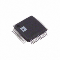
AD9753ASTZ Analog Devices Inc, AD9753ASTZ Datasheet - Page 4

AD9753ASTZ
Manufacturer Part Number
AD9753ASTZ
Description
12-Bit, 300 MSPS TxDAC+ DAC
Manufacturer
Analog Devices Inc
Series
TxDAC+®r
Datasheet
1.AD9753ASTZ.pdf
(28 pages)
Specifications of AD9753ASTZ
Settling Time
11ns
Number Of Bits
12
Data Interface
Parallel
Number Of Converters
1
Voltage Supply Source
Analog and Digital
Power Dissipation (max)
165mW
Operating Temperature
-40°C ~ 85°C
Mounting Type
Surface Mount
Package / Case
48-LQFP
Number Of Channels
1
Resolution
12b
Interface Type
Parallel
Single Supply Voltage (typ)
3.3V
Dual Supply Voltage (typ)
Not RequiredV
Architecture
Segment
Power Supply Requirement
Analog and Digital
Output Type
Current
Single Supply Voltage (min)
3V
Single Supply Voltage (max)
3.6V
Dual Supply Voltage (min)
Not RequiredV
Dual Supply Voltage (max)
Not RequiredV
Operating Temp Range
-40C to 85C
Operating Temperature Classification
Industrial
Mounting
Surface Mount
Pin Count
48
Package
48LQFP
Conversion Rate
300 MSPS
Digital Interface Type
Parallel
Number Of Outputs Per Chip
1
Full Scale Error
±2 %FSR
Integral Nonlinearity Error
±1.5 LSB
Maximum Settling Time
0.011(Typ) us
Lead Free Status / RoHS Status
Lead free / RoHS Compliant
For Use With
AD9753-EB - BOARD EVAL FOR AD9753
Lead Free Status / Rohs Status
Compliant
Available stocks
Company
Part Number
Manufacturer
Quantity
Price
Company:
Part Number:
AD9753ASTZ
Manufacturer:
Analog Devices Inc
Quantity:
10 000
Part Number:
AD9753ASTZ
Manufacturer:
ADI/亚德诺
Quantity:
20 000
Company:
Part Number:
AD9753ASTZRL
Manufacturer:
Analog Devices Inc
Quantity:
10 000
AD9753
DIGITAL SPECIFICATIONS
Parameter
DIGITAL INPUTS
CLK INPUTS
*Min CLK Frequency applies only when using internal PLL. When PLL is disabled, there is no minimum CLK frequency.
Specifications subject to change without notice.
Logic 1
Logic 0
Logic 1 Current
Logic 0 Current
Input Capacitance
Input Setup Time (t
Input Hold Time (t
Latch Pulsewidth (t
Input Setup Time (t
Input Hold Time (t
CLK to PLLLOCK Delay (t
Latch Pulsewidth (t
PLLOCK (V
PLLOCK (V
Input Voltage Range
Common-Mode Voltage
Differential Voltage
Min CLK Frequency*
OH
OL
)
)
H
H
LPW
LPW
S
S
), T
, PLLVDD = 0 V), T
), T
, PLLVDD = 0 V), T
), T
PLLVDD = 0 V), T
A
A
= 25°C
= 25°C
A
D
= 25°C
, PLLVDD = 0 V), T
(T
MIN
to T
A
A
A
= 25°C
= 25°C
MAX
= 25°C
, AVDD = DVDD = PLLVDD = CLKVDD = 3.3 V, I
A
= 25°C
–4–
Min
2.1
–10
–10
1.0
1.0
1.5
–1.0
2.5
3.5
1.5
3.0
0
0.75
0.5
Typ
3
0
5
0.5
0.5
–1.5
1.7
1.5
1.5
6.25
OUTFS
= 20 mA, unless otherwise noted.)
Max
0.9
+10
+10
4.0
0.3
3
2.25
Unit
V
V
µA
µA
pF
ns
ns
ns
ns
ns
ns
ns
V
V
V
V
V
MHz
REV. B


