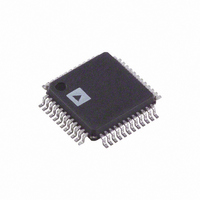
AD9753ASTZ Analog Devices Inc, AD9753ASTZ Datasheet - Page 16

AD9753ASTZ
Manufacturer Part Number
AD9753ASTZ
Description
12-Bit, 300 MSPS TxDAC+ DAC
Manufacturer
Analog Devices Inc
Series
TxDAC+®r
Datasheet
1.AD9753ASTZ.pdf
(28 pages)
Specifications of AD9753ASTZ
Settling Time
11ns
Number Of Bits
12
Data Interface
Parallel
Number Of Converters
1
Voltage Supply Source
Analog and Digital
Power Dissipation (max)
165mW
Operating Temperature
-40°C ~ 85°C
Mounting Type
Surface Mount
Package / Case
48-LQFP
Number Of Channels
1
Resolution
12b
Interface Type
Parallel
Single Supply Voltage (typ)
3.3V
Dual Supply Voltage (typ)
Not RequiredV
Architecture
Segment
Power Supply Requirement
Analog and Digital
Output Type
Current
Single Supply Voltage (min)
3V
Single Supply Voltage (max)
3.6V
Dual Supply Voltage (min)
Not RequiredV
Dual Supply Voltage (max)
Not RequiredV
Operating Temp Range
-40C to 85C
Operating Temperature Classification
Industrial
Mounting
Surface Mount
Pin Count
48
Package
48LQFP
Conversion Rate
300 MSPS
Digital Interface Type
Parallel
Number Of Outputs Per Chip
1
Full Scale Error
±2 %FSR
Integral Nonlinearity Error
±1.5 LSB
Maximum Settling Time
0.011(Typ) us
Lead Free Status / RoHS Status
Lead free / RoHS Compliant
For Use With
AD9753-EB - BOARD EVAL FOR AD9753
Lead Free Status / Rohs Status
Compliant
Available stocks
Company
Part Number
Manufacturer
Quantity
Price
Company:
Part Number:
AD9753ASTZ
Manufacturer:
Analog Devices Inc
Quantity:
10 000
Part Number:
AD9753ASTZ
Manufacturer:
ADI/亚德诺
Quantity:
20 000
Company:
Part Number:
AD9753ASTZRL
Manufacturer:
Analog Devices Inc
Quantity:
10 000
AD9753
and is insensitive to f
both the digital input waveform, f
DVDD. Figure 18 shows I
f
effect that the speed of f
the PLL divider ratio.
DAC
) for various update rates. In addition, Figure 19 shows the
40
35
30
25
20
15
10
10
9
8
7
6
5
4
3
2
1
0
5
0
20
18
16
14
12
10
0.001
8
6
4
2
0
0
0
DIV SETTING 11
25
Figure 18. I
2.5
50
Figure 19. PLLVDD vs. f
Figure 17. I
CLOCK
5.0
75
DAC
100
0.01
DIV SETTING 10
DVDD
DVDD
. Conversely, I
7.5
RATIO
has on the PLLVDD current, given
125
I
f
OUTFS
DAC
AVDD
vs. f
as a function of the ratio (f
10.0
150
100MSPS
200MSPS
(f
300MSPS
50MSPS
25MSPS
(MHz)
OU T
(mA)
CLOCK
vs. I
OUT
175
/
f
DAC
12.5
DIV SETTING 01
/f
200
)
OUTFS
0.1
DAC
, and digital supply,
DVDD
DIV SETTING 00
DAC
15.0
225
Ratio
is dependent on
250
17.5
275
20.0
300
1
OUT
/
–16–
APPLYING THE AD9753
OUTPUT CONFIGURATIONS
The following sections illustrate some typical output configura-
tions for the AD9753. Unless otherwise noted, it is assumed
that I
ing the optimum dynamic performance, a differential output
configuration is suggested. A differential output configuration
may consist of either an RF transformer or a differential op amp
configuration. The transformer configuration provides the opti-
mum high frequency performance and is recommended for any
application allowing for ac coupling. The differential op amp
configuration is suitable for applications requiring dc coupling,
a bipolar output, signal gain, and/or level shifting, within the
bandwidth of the chosen op amp.
A single-ended output is suitable for applications requiring a
unipolar voltage output. A positive unipolar output voltage will
result if I
sized load resistor, R
ration may be more suitable for a single-supply system requiring
a dc-coupled, ground referred output voltage. Alternatively, an
amplifier could be configured as an I-V converter, thus con-
verting I
configuration provides the best dc linearity since I
is maintained at a virtual ground. Note that I
slightly better performance than I
DIFFERENTIAL COUPLING USING A TRANSFORMER
An RF transformer can be used to perform a differential-to-
single-ended signal conversion, as shown in Figure 20. A
differentially-coupled transformer output provides the optimum
distortion performance for output signals whose spectral content
lies within the transformer’s pass band. An RF transformer such
as the Mini-Circuits T1-1T provides excellent rejection of
common-mode distortion (i.e., even-order harmonics) and noise
over a wide frequency range. When I
nated to ground with 50 Ω, this configuration provides 0 dBm
power to a 50 Ω load on the secondary with a DAC full-scale
current of 20 mA. A 2:1 transformer, such as the Coilcraft
WB2040-PC, can also be used in a configuration in which I
and I
tion improves load matching and increases power to 2 dBm into
a 50 Ω load on the secondary. Transformers with different imped-
ance ratios may also be used for impedance matching purposes.
Note that the transformer provides ac coupling only.
The center tap on the primary side of the transformer must
be connected to ACOM to provide the necessary dc current
path for both I
appearing at I
symmetrically around ACOM and should be maintained with
the specified output compliance range of the AD9753. A differ-
ential resistor, R
output of the transformer is connected to the load, R
Figure 20. Differential Output Using a Transformer
OUTB
OUTFS
OUTA
OUTA
are terminated to ground with 75 Ω. This configura-
is set to a nominal 20 mA. For applications requir-
AD9753
or I
OUTA
and/or I
OUTA
DIFF
I
I
OUTA
OUTB
OUTB
and I
, may be inserted in applications where the
and I
LOAD
OUTB
into a negative unipolar voltage. This
OUTB
, referred to ACOM. This configu-
OUTB
is connected to an appropriately
(i.e., V
. The complementary voltages
OUTB
MINI-CIRCUITS
OUTA
T1-1T
.
OUTA
and I
and V
OUTA
OUTB
OUTA
R
OUTB
LOAD
provides
are termi-
LOAD
) swing
or I
REV. B
, via a
OUTB
OUTA


