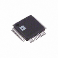
AD1970JSTZRL Analog Devices Inc, AD1970JSTZRL Datasheet - Page 8

AD1970JSTZRL
Manufacturer Part Number
AD1970JSTZRL
Description
IC,TV/VIDEO CIRCUIT,TV Stereo Circuit,QFP,48PIN,PLASTIC
Manufacturer
Analog Devices Inc
Type
Audio Encoderr
Datasheet
1.AD1970JSTZRL.pdf
(20 pages)
Specifications of AD1970JSTZRL
Applications
Set-Top Boxes, Video Players, Recorders
Voltage - Supply, Analog
3 V ~ 3.6 V
Voltage - Supply, Digital
3 V ~ 3.6 V
Mounting Type
Surface Mount
Package / Case
48-LQFP
Lead Free Status / RoHS Status
Lead free / RoHS Compliant
For Use With
EVAL-AD1970EB - BOARD EVALUATION FOR AD1970
Lead Free Status / RoHS Status
Lead free / RoHS Compliant
Available stocks
Company
Part Number
Manufacturer
Quantity
Price
Company:
Part Number:
AD1970JSTZRL
Manufacturer:
Analog Devices Inc
Quantity:
10 000
AD1970
Pin No.
18
19
20
21
22
23
24
25
26
27
28
29
30
31
32
33
34
35
36
37
38
39
40
41
42
43
44
45
46
47
48
Pin Name
VIN_IAMPR
CAPLP
CAPLN
CAPRP
CAPRN
PVDD
PLL_LF
PGND
VID_IN
NC
PLL_MODE0
PLL_MODE1
MCLK
VID_PRES
XOUT
XIN
GPIO0
GPIO1
DGND
DVDD
GPIO2
GPIO3
SDATA
BCLK
LRCLK
DIG_IN_EN
SDA
SCL
ADR1
ADR0
DGND
IN
I/O
I/O
I/O
I/O
IN
IN
IN
OUT
OUT
IN
IN/OUT
IN/OUT
IN/OUT
IN/OUT
IN/OUT
IN/OUT
IN
IN/OUT
IN
IN
IN
Input/Output
IN
IN/OUT
Description
Negative input of internal op amp for right channel input amplifier.
ADC Filter Capacitor Connection (positive left-channel input to modulator). A 1 nF
capacitor should be placed between this pin and analog ground.
ADC Filter Capacitor Connection (negative left-channel input to modulator). A 1 nF
capacitor should be placed between this pin and analog ground.
ADC Filter Capacitor Connection (positive right-channel input to modulator). A 1 nF
capacitor should be placed between this pin and analog ground.
ADC Filter Capacitor Connection (negative right-channel input to modulator). A 1 nF
capacitor should be placed between this pin and analog ground.
PLL Power. 3.3 V nominal. Bypass capacitors should be placed close to this pin and
connected directly to the PLL ground.
PLL Loop Filter Connection.
PLL Ground. Connect to DGND.
Composite Video Input. Composite video signal input to the sync separator. The sync
output is connected to a PLL that generates the clocks for the AD1970. This pin has an
input impedance of 2 kΩ.
No Connect.
PLL Mode Select Pin 0. The setting of these pins indicates the source and frequency of the
input clock to generate the internal MCLK for the AD1970.
PLL Mode Select Pin 1. The setting of these pins indicates the source and frequency of the
input clock to generate the internal MCLK for the AD1970.
Master Clock Input. This input is used to generate the internal master clock if it is not
derived from the composite video signal on VID_IN. The master clock frequency must be
either fs or 256 × fs, where fs is the input sampling frequency. The PLL_CTRLx pins should
be set to accept the appropriate MCLK input frequency.
Video Present Flag. A high logic level on this pin indicates that a valid composite video
signal is present on the VID_IN pin. Open-drain output.
Crystal Oscillator Output. This pin is the output of the on-board oscillator and should be
connected to one side of a crystal.
Crystal Oscillator Input. This pin is the input to the on-board oscillator and should be
connected to one side of a crystal.
General Purpose I/O 0. This pin can be set to be either a static input or output, with levels
and direction controlled through the I
General Purpose I/O 1. This pin can be set to be either a static input or output, with levels
and direction controlled through the I
Digital Ground.
Digital Power.
General Purpose I/O 2. This pin can be set to be either a static input or output, with levels
and direction controlled through the I
General Purpose I/O 3. This pin can be set to be either a static input or output, with levels
and direction controlled through the I
Serial Data Input/Output (Before BTSC Encoding). Digital input to the BTSC encoder or
output of the ADC. The serial format is selected by writing to Bits 3:2 of Control Register 1.
Bit Clock Input/Output. Serial bit clock for clocking in the serial data. The interpretation of
BCLK changes according to the serial mode, which is set by writing to the control
registers.
Left/Right Clock Input/Output. Left/right clock for framing the serial input data. The
interpretation of the LRCLK changes according to the serial mode, set by writing to the
control registers.
Digital Input Enable (active high).
I
I
I
I
Digital Ground.
2
2
2
2
C Serial Data Input/Output.
C Serial Clock Input.
C Address 1. The address of the I
C Address 0. The address of the I
Rev. 0 | Page 8 of 20
2
2
C port is set by these pins according to Table 16.
C port is set by these pins according to Table 16.
2
2
2
2
C port.
C port.
C port.
C port.


