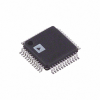
AD1970JSTZRL Analog Devices Inc, AD1970JSTZRL Datasheet - Page 14

AD1970JSTZRL
Manufacturer Part Number
AD1970JSTZRL
Description
IC,TV/VIDEO CIRCUIT,TV Stereo Circuit,QFP,48PIN,PLASTIC
Manufacturer
Analog Devices Inc
Type
Audio Encoderr
Datasheet
1.AD1970JSTZRL.pdf
(20 pages)
Specifications of AD1970JSTZRL
Applications
Set-Top Boxes, Video Players, Recorders
Voltage - Supply, Analog
3 V ~ 3.6 V
Voltage - Supply, Digital
3 V ~ 3.6 V
Mounting Type
Surface Mount
Package / Case
48-LQFP
Lead Free Status / RoHS Status
Lead free / RoHS Compliant
For Use With
EVAL-AD1970EB - BOARD EVALUATION FOR AD1970
Lead Free Status / RoHS Status
Lead free / RoHS Compliant
Available stocks
Company
Part Number
Manufacturer
Quantity
Price
Company:
Part Number:
AD1970JSTZRL
Manufacturer:
Analog Devices Inc
Quantity:
10 000
AD1970
Dialog Enhancement Register
This controls the built-in dialog enhancement algorithm, and
defaults to 0. The maximum setting is 0100000000000000000000
or a twos complement fractional value of 1.0. This algorithm is
intended to solve the problem of playing back high dynamic
range digital audio signals over a television’s built-in speakers. It
provides an amplitude boost to signals that are in the range
where dialog signals are usually found, while at the same time
preventing loud special effects passages from overloading the
speakers or amplifiers.
(CONTINUED)
(CONTINUED)
(CONTINUED)
(CONTINUED)
SDA
SDA
SDA
SCL
SCL
SCL
START BY
MASTER
SDA
SCL
REPEATED START
BY MASTER
START BY
MASTER
D15 D14 D13 D12 D11 D10
0
0
0
1
REGISTER DATA UPPER BYTE
1
1
CHIP ADDRESS BYTE
0
CHIP ADDRESS BYTE
CHIP ADDRESS BYTE
0
0
FRAME 1
0
FRAME 4
FRAME 1
FRAME 4
0
0
0
0
0
AD1
AD1 AD0
AD1 AD0
AD0
D9
Figure 4. Sample of I
Figure 5. Sample of I
WRITE
R/W
I
WRITE
2
D8
READ
C
I
R/W
R/W
2
I
2
C
C
ACK. BY
AD1970
ACK. BY
AD1970
ACK. BY
ACK. BY
AD1970
AD1970
D7
0
D7
0
REGISTER ADDRESS UPPER BYTE
D6
2
2
Rev. 0 | Page 14 of 20
0
REGISTER DATA LOWER BYTE
C Write Format (Control Register 1 Write)
C Read Format (Control Register 1 Read)
REGISTER ADDRESS UPPER BYTE
D6
0
D5
0
D5
REGISTER DATA BYTE
0
D4
FRAME 5
0
FRAME 2
D4
0
FRAME 2
FRAME 5
D3
0
I
The read/write formats of the I
oriented. This allows for easy programming of common micro-
controller chips. In order to fit into a byte oriented format, 0s
are appended to the data fields in order to extend the data word
to the next multiple of 8 bits. For example, 22-bit words written
to the parameter RAM are appended with two leading zeroes in
order to reach 24 bits (3 bytes). These zero-extended data fields
are appended to a 2-byte field consisting of a read/write bit and
a 10-bit address. The I
expect based on the address received in the first two bytes.
D3
REGISTER
0
2
REGISTER
C READ/WRITE DATA FORMATS
WRITE
R/W
READ
R/W
D2
D2
0
D1
D1
0
D0
1
D0
1
ACK. BY
ACK. BY
ACK. BY
MASTER
AD1970
ACK. BY
AD1970
AD1970
0
0
2
STOP BY
MASTER
STOP BY
MASTER
C port knows how many data bytes to
REGISTER ADDRESS LOWER BYTE
REGISTER ADDRESS LOWER BYTE
0
0
0
0
2
C port are designed to be byte
0
FRAME 3
0
FRAME 3
0
0
0
0
0
0
1
1
ACK. BY
AD1970
ACK. BY
AD1970


