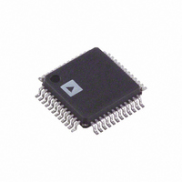
AD1970JSTZRL Analog Devices Inc, AD1970JSTZRL Datasheet - Page 7

AD1970JSTZRL
Manufacturer Part Number
AD1970JSTZRL
Description
IC,TV/VIDEO CIRCUIT,TV Stereo Circuit,QFP,48PIN,PLASTIC
Manufacturer
Analog Devices Inc
Type
Audio Encoderr
Datasheet
1.AD1970JSTZRL.pdf
(20 pages)
Specifications of AD1970JSTZRL
Applications
Set-Top Boxes, Video Players, Recorders
Voltage - Supply, Analog
3 V ~ 3.6 V
Voltage - Supply, Digital
3 V ~ 3.6 V
Mounting Type
Surface Mount
Package / Case
48-LQFP
Lead Free Status / RoHS Status
Lead free / RoHS Compliant
For Use With
EVAL-AD1970EB - BOARD EVALUATION FOR AD1970
Lead Free Status / RoHS Status
Lead free / RoHS Compliant
Available stocks
Company
Part Number
Manufacturer
Quantity
Price
Company:
Part Number:
AD1970JSTZRL
Manufacturer:
Analog Devices Inc
Quantity:
10 000
PIN CONFIGURATION AND FUNCTION DESCRIPTIONS
Table 13. Pin Function Descriptions
Pin No.
1
2
3
4
5
6
7
8
9
10
11
12
13
14
15
16
17
Pin Name
DVDD
RESETB
DGND
DVDD
RSVD
VOUT_OAMP
VIN_OAMP
AVDD
BTSC_OUT
AGND
VREF
FILTCAP
AVDD
AGND
VOUT_IAMPL
VIN_IAMPL
VOUT_IAMPR
Input/Output
IN
OUT
IN
OUT
OUT
OUT
OUT
IN
OUT
VOUT_OAMP
BTSC_OUT
VIN_OAMP
FILTCAP
RESETB
DGND
AGND
DVDD
DVDD
RSVD
AVDD
VREF
Description
Digital Power.
Reset—Active Low. After RESETB transitions from low to high, the AD1970 BTSC encoder
core goes through an initialization sequence where all registers are set to 0. The
initialization is completed after 1024 MCLK cycles. New values should not be written to
the control port until the initialization is complete.
Digital Ground.
Digital Power. 3.3 V nominal.
Reserved—Connect to DGND.
Output voltage of internal op amp to be used for BTSC output low pass filter.
Negative input of internal op amp to be used for BTSC output low pass filter.
Analog Power.
Encoded BTSC Output. The nominal output voltage for a 300 Hz, 0 dB mono input signal is
250 mV rms.
Analog Ground.
Connection for voltage reference noise reduction capacitor. The nominal VREF voltage is
1.5 V; the analog gain scales directly with the voltage on this pin. Any ac signal on this pin
causes distortion and therefore a large decoupling capacitor should be used to ensure the
voltage on VREF is clean.
Connection for DAC noise reduction capacitor. A 10 µF capacitor should be connected to
this pin to reduce the noise on an internal DAC biasing point to provide the highest
performance. It may not be necessary to connect this pin, depending on the quality of the
layout and grounding used in the application circuit.
Analog Power. 3.3 V nominal. Bypass capacitors should be placed close to the pins and
connected directly to the analog ground plane.
Analog Ground.
Output of internal op amp for left channel input amplifier.
Negative input of internal op amp for left channel input amplifier.
Output of internal op amp for right channel input amplifier.
10
11
12
1
2
3
4
5
6
7
8
9
48 47 46 45 44 43 42 41 40 39 38 37
13 14 15 16 17 18 19 20 21 22 23 24
Figure 2. Pin Configuration
Rev. 0 | Page 7 of 20
NC = NO CONNECT
(Not to Scale)
AD1970
TOP VIEW
36
35
34
33
32
31
30
29
28
27
26
25
DGND
GPIO1
GPIO0
XIN
XOUT
VID_PRES
MCLK
PLL_MODE1
PLL_MODE0
NC
VID_IN
PGND
AD1970


