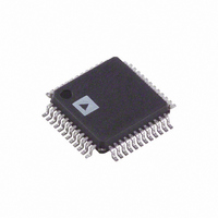
AD1970JSTZRL Analog Devices Inc, AD1970JSTZRL Datasheet - Page 12

AD1970JSTZRL
Manufacturer Part Number
AD1970JSTZRL
Description
IC,TV/VIDEO CIRCUIT,TV Stereo Circuit,QFP,48PIN,PLASTIC
Manufacturer
Analog Devices Inc
Type
Audio Encoderr
Datasheet
1.AD1970JSTZRL.pdf
(20 pages)
Specifications of AD1970JSTZRL
Applications
Set-Top Boxes, Video Players, Recorders
Voltage - Supply, Analog
3 V ~ 3.6 V
Voltage - Supply, Digital
3 V ~ 3.6 V
Mounting Type
Surface Mount
Package / Case
48-LQFP
Lead Free Status / RoHS Status
Lead free / RoHS Compliant
For Use With
EVAL-AD1970EB - BOARD EVALUATION FOR AD1970
Lead Free Status / RoHS Status
Lead free / RoHS Compliant
Available stocks
Company
Part Number
Manufacturer
Quantity
Price
Company:
Part Number:
AD1970JSTZRL
Manufacturer:
Analog Devices Inc
Quantity:
10 000
AD1970
CONTROL PORT
I
The AD1970 can be controlled using the I
there are three parameters that can be controlled: the encoder
output level, the Phat Stereo image enhancement algorithm, and
the dialog enhancement algorithm. It is also possible to write
new data into the parameter RAM to alter the filter coefficients
used in the BTSC encoding process. Since this is a fairly
complex topic and is unnecessary for normal operation of the
chip, the details are not included in this data sheet; please
contact ADI sales if modifications to the BTSC filters are
required.
The I
bidirectional data line, and SCL, the clock.
The R/ W bit is low for a write operation and high for a read
operation. The 10-bit address word is decoded into either a
location in the parameter RAM or one of the registers. The
Table 17. I
Register Address
0
1 to 254
255
256
257
258
259
260
2
C PORT OVERVIEW
2
C port uses a 2-wire interface consisting of SDA, the
2
C Port Address Decoding
Register Name
Input Level Control
Parameter RAM
Output Level Control
Control Register 1
Control Register 2
ADC Volume Control
Stereo Spreading Control
Dialog Enhancement Control
2
C port. In general,
Rev. 0 | Page 12 of 20
number of data bytes varies according to the register or
memory being accessed. The detailed data format diagram for
continuous-mode operation is given in the section.
I
Table 16 shows the address decoding used in the I
different addresses are available to avoid conflicting addresses
on an I
registers and the parameter RAM. The parameter RAM is
loaded on power-up from an on-board boot ROM.
Table 16. I
ADR1
0
0
1
1
2
C ADDRESS DECODING
2
C bus. The I
2
C Address Settings
Read/Write Word Length
Write: 22 bits
Read: 22 bits
Write: 11 bits
Read: 6 bits
Write: 22 bits
ADR0
0
1
0
1
2
C address space encompasses a set a
I
0x20
0x21
0x22
0x23
2
C Address
2
C port. Four


