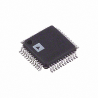
AD1970JSTZRL Analog Devices Inc, AD1970JSTZRL Datasheet - Page 11

AD1970JSTZRL
Manufacturer Part Number
AD1970JSTZRL
Description
IC,TV/VIDEO CIRCUIT,TV Stereo Circuit,QFP,48PIN,PLASTIC
Manufacturer
Analog Devices Inc
Type
Audio Encoderr
Datasheet
1.AD1970JSTZRL.pdf
(20 pages)
Specifications of AD1970JSTZRL
Applications
Set-Top Boxes, Video Players, Recorders
Voltage - Supply, Analog
3 V ~ 3.6 V
Voltage - Supply, Digital
3 V ~ 3.6 V
Mounting Type
Surface Mount
Package / Case
48-LQFP
Lead Free Status / RoHS Status
Lead free / RoHS Compliant
For Use With
EVAL-AD1970EB - BOARD EVALUATION FOR AD1970
Lead Free Status / RoHS Status
Lead free / RoHS Compliant
Available stocks
Company
Part Number
Manufacturer
Quantity
Price
Company:
Part Number:
AD1970JSTZRL
Manufacturer:
Analog Devices Inc
Quantity:
10 000
SEPARATION ALIGNMENT
The BTSC encoder outputs are all specified in terms of the
deviation of the FM 4.5 MHz carrier. For the AD1970, a digital
input level of 0 dB (mono signal) should cause a carrier devia-
tion of ±25 kHz without the 75 µs pre-emphasis filter. In
practice, the pre-emphasis filter can be left in for this adjust-
ment, as long as the frequency is low enough to not be affected
by the filter. It is critical to maintain the proper gain relationship
between the BTSC encoder and the 4.5 MHz FM modulator. A
common mistake is to assume that changing the gain between
the BTSC encoder output and the FM modulator input has the
same effect as changing the audio input level going in to the
BTSC encoder. The presence of a complicated 2-band nonlinear
dynamics processor means that the encoder output must be
connected to the decoder input (through the FM modulation/
demodulation process) with a known gain. If this gain is
changed, then the separation significantly suffers.
When measuring the AD1970 on the bench, it is possible to use
a BTSC reference decoder box, so that the FM modulation/
demodulation process can be skipped. These units have a
method of adjusting the input voltage sensitivity to achieve best
separation. The output level of the AD1970 can also be adjusted
over a wide range using either the I
adjusting the values of the components used in the external
analog low-pass filter that is between the BTSC encoder output
and the input to the FM modulator.
PHASE LINEARITY OF THE EXTERNAL ANALOG
FILTER
If the time-alignment of the pilot to the carrier signal is not
close to 0°, a loss of separation can occur. This means that the
external analog low-pass filter should be a linear-phase design
to provide constant group delay over the range from dc to
50 kHz. A Bessel filter is recommended for this application. The
typical applications circuit (see Figure 8) shows a recommended
design for this filter.
INPUT LEVELS
The maximum input level to the AD1970 changes across
frequency. Table 14 shows the maximum allowable input level
for different frequencies. These values are part of the BTSC
specification, not a function of this chip.
2
C control port or by
Rev. 0 | Page 11 of 20
Table 14. Maximum Input Levels to the BTSC Encoder
across Frequency
Frequency (Hz)
20 to 1000
1600
2500
3150
5000
8000
12500
CLOCKING AND PLL
The AD1970’s master clock either can be directly fed to the
MCLK pin or generated by a PLL from a composite video signal
input on the VID_IN pin. If the clock input is on the MCLK pin,
the PLL can synthesize the internal clocks from either a clock at
the digital audio frame sync frequency (f
The PLL mode is controlled by Pins PLL_MODE0 and
PLL_MODE1. The settings are shown in Table 15.
Table 15. PLL Modes
PLL_MODE1
0
0
1
1
CRYSTAL OSCILLATOR
The AD1970 has an on-board crystal oscillator to generate a
clock that can be used by an RF modulator or other application.
For example, a 4 MHz crystal can be connected as shown in the
application circuit (see Figure 8). The AD1970 does not use this
clock itself, so if it is not needed in an application the XIN pin
should be grounded and the XOUT pin left unconnected.
GENERAL PURPOSE INPUT/OUTPUT (GPIO) PINS
Pins GPIO0, GPIO1, GPIO2, and GPIO3 are set to be inputs or
outputs by Bits 19:16 of Control Register 2. All four default to
input state. These pins do not take an input to or send an output
from the main signal flow. When set as an output, the binary
value on the pins is set according to Bits 15:12 of Control
Register 2. These pins can be used to interface with I/O pins on
a microcontroller and allow hardware control via the I
POWER-UP SEQUENCE
The AD1970 has a built-in power-up sequence that initializes
the contents of all internal RAMs. During this time, the
parameter RAM is filled with values from its associated boot
ROM. The data memories are also cleared during this time.
The boot sequence lasts for 1024 MCLK cycles and starts on the
rising edge of the RESETB pin. The user should avoid writing to
or reading from the I
PLL_MODE0
0
1
0
1
2
C registers during this period of time.
Maximum Input Level (dBFS)
0
−1
−3
−5
−8
−11
−15
Setting
Composite video input (on
VID_IN)
256 × fs (on MCLK)
fs (on MCLK)
PLL bypass
S
= 48 kHz) or 256 × f
AD1970
2
C bus.
S
.


