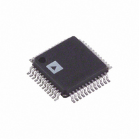
AD1970JSTZRL Analog Devices Inc, AD1970JSTZRL Datasheet - Page 16

AD1970JSTZRL
Manufacturer Part Number
AD1970JSTZRL
Description
IC,TV/VIDEO CIRCUIT,TV Stereo Circuit,QFP,48PIN,PLASTIC
Manufacturer
Analog Devices Inc
Type
Audio Encoderr
Datasheet
1.AD1970JSTZRL.pdf
(20 pages)
Specifications of AD1970JSTZRL
Applications
Set-Top Boxes, Video Players, Recorders
Voltage - Supply, Analog
3 V ~ 3.6 V
Voltage - Supply, Digital
3 V ~ 3.6 V
Mounting Type
Surface Mount
Package / Case
48-LQFP
Lead Free Status / RoHS Status
Lead free / RoHS Compliant
For Use With
EVAL-AD1970EB - BOARD EVALUATION FOR AD1970
Lead Free Status / RoHS Status
Lead free / RoHS Compliant
Available stocks
Company
Part Number
Manufacturer
Quantity
Price
Company:
Part Number:
AD1970JSTZRL
Manufacturer:
Analog Devices Inc
Quantity:
10 000
AD1970
ANALOG INPUT/OUTPUT
ADC INPUT
The AD1970 accepts an analog left-right signal on its input.
DAC OUTPUT
Figure 6 shows the block diagram of the analog output. A series
of current sources are controlled by a digital Σ-Δ modulator.
Depending on the digital code from the modulator, each cur-
rent source is connected to the summing junction of either a
positive I-to-V converter or a negative I-to-V converter. Two
extra current sources that push instead of pull are added to set
the midscale common-mode voltage.
All current sources are derived from the VREF input pin. The
gain of the AD1970 is directly proportional to the magnitude of
the current sources, and therefore the gain of the AD1970 is
proportional to the voltage generated on the VREF pin. The
nominal VREF voltage is 1.5 V.
Since the VREF input effectively multiplies the signal, care must
be taken to insure that no ac signals appear on this pin. This can
be accomplished by using a large decoupling capacitor con-
nected to VREF.
The AD1970 should be used with an external third order filter
on each output channel, as shown in Figure 8. The values shown
are for a 100 kHz Bessel filter. The use of a Bessel filter is impor-
tant to maintain the time-alignment of the pilot to the carrier. If
these signals are not in phase, a loss of separation occurs.
For best performance, a large (>10 µF) capacitor should be
connected between the FILTCAP pin and analog ground.
Σ–∆ MODULATOR
FROM DIGITAL
OUT+
(DIG_IN)
I
REF
Figure 6. Internal DAC Analog Architecture
+ DIG_IN
I
REF
SWITCHED CURRENT
SOURCES
BIAS
V
REF
IN
I
REF
I
REF
– DIG_IN
OUT–
Rev. 0 | Page 16 of 20
SERIAL DATA PORT
The AD1970’s flexible serial audio interface accepts and sends
data in twos complement, MSB first format. The left channel
data field always precedes the right channel data field. The serial
mode is set by using mode select bits in the control register. In
all modes except for the right justified mode, the serial port
accepts an arbitrary number of bits up to a limit of 24 (extra bits
do not cause an error, but they are truncated internally). In the
right-justified mode, control register bits are used to set the
word length to 16, 20, or 24 bits. The default on power-up is 24-
bit mode. Proper operation of the right justified mode requires
that there be exactly 64 BCLKs per audio frame.
SERIAL DATA MODES
Figure 7 shows the left-justified mode. LRCLK is high for the
left channel, and low for the right channel. Data is sampled on
the rising edge of BCLK. The MSB is left-justified to a LRCLK
transition, with no MSB delay. The left-justified mode can
accept any word length up to 24 bits.
Figure 7 shows the I2S mode, which is the default setting.
LRCLK is low for the left channel and the MSB is delayed from
the edge of the LRCLK by a single BCLK period. The I2S mode
can be used to accept any number of bits up to 24.
Figure 7 shows the right-justified mode of the AD1970. LRCLK
is high for the left channel, low for the right channel. Data is
sampled on the rising edge of BCLK. The start of data is delayed
from the LRCLK edge by 16, 12, or 8 BCLK intervals, depending
on the selected word length. The default word length is 24 bits;
other word lengths are set by writing to Bits 1:0 of the control
register. In right-justified mode, it is assumed that there are 64
BCLKs per frame.
Figure 7 shows the DSP serial port mode. LRCLK must pulse
high for at least one bit clock period before the MSB of the left
channel is valid and LRCLK must pulse high again for at least
one bit clock period before the MSB of the right channel is
valid. Data is sampled on the falling edge of BCLK. The DSP
serial port mode can be used with any word length up to 24 bits.
In this mode, it is the responsibility of the DSP to ensure that
the left data is transmitted with the first LRCLK pulse and that
synchronism is maintained from that point forward.


