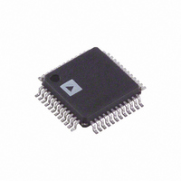
AD1970JSTZRL Analog Devices Inc, AD1970JSTZRL Datasheet - Page 13

AD1970JSTZRL
Manufacturer Part Number
AD1970JSTZRL
Description
IC,TV/VIDEO CIRCUIT,TV Stereo Circuit,QFP,48PIN,PLASTIC
Manufacturer
Analog Devices Inc
Type
Audio Encoderr
Datasheet
1.AD1970JSTZRL.pdf
(20 pages)
Specifications of AD1970JSTZRL
Applications
Set-Top Boxes, Video Players, Recorders
Voltage - Supply, Analog
3 V ~ 3.6 V
Voltage - Supply, Digital
3 V ~ 3.6 V
Mounting Type
Surface Mount
Package / Case
48-LQFP
Lead Free Status / RoHS Status
Lead free / RoHS Compliant
For Use With
EVAL-AD1970EB - BOARD EVALUATION FOR AD1970
Lead Free Status / RoHS Status
Lead free / RoHS Compliant
Available stocks
Company
Part Number
Manufacturer
Quantity
Price
Company:
Part Number:
AD1970JSTZRL
Manufacturer:
Analog Devices Inc
Quantity:
10 000
INPUT LEVEL CONTROL
This register location controls the input level of both the left
and right channels to the AD1970 BTSC encoding algorithm.
The register defaults to a value of 1.0 (0100000000000000000000
in binary 2.20 format) and allows a maximum of 12 dB of gain
at a full-scale value. This feature allows compatibility with the
Dolby digital specification for proper operation in both RF
mode and line mode. In RF mode, the dialog level is specified at
11 dB higher than the dialog level in line mode. A gain of 11 dB
can be achieved by writing 1.8836 to Address 0.
OUTPUT LEVEL CONTROL
The level control of the BTSC-encoded output is controlled
in this register location. The default value is 0.5 (–6 dB,
0010000000000000000000 in binary 2.20 format), or 250 mV
on the DAC output. The output level should not be used as a
volume control. Its intended use, in conjunction with the output
filter, is to match the level with the expected input of the BTSC
decoder. Matching these allows maximum separation between
the left and right encoded channels.
Control Register 1
Control Register 1 is an 11-bit register that controls serial
modes, de-emphasis, mute, power-down, and I
transfers. Table 18 documents the contents of this register.
Bits 5:4 and 10:8 are reserved and should be set to 0 at all times.
The audio signal is muted with Bit 7 of the control register.
The soft power-down bit (Bit 6) stops the internal clocks to the
DSP core, but does not reset the part. The digital power
consumption is reduced to a low level when this bit is asserted.
Reset can only be asserted using the external reset pin.
Bits 3:2 select the serial format from one of four modes. These
different formats are discussed in the section of this data sheet.
The word length bits (1:0) are used in right-justified serial
modes to determine where the MSB is located relative to the
start of the audio frame.
2
C-to-memory
Rev. 0 | Page 13 of 20
Table 18. Control Register 1 Write
Register Bits
10:8
7
6
5:4
3:2
1:0
Table 19. Control Register 1 Read
Register Bits
5:2
1:0
Control Register 2
Control Register 2 is a 22-bit write-only register that controls
power down modes, PLL and sync separator controls, and
digital I/O pin functions.
Table 20. Control Register 2
Register Bits
21
20
19:16
15:12
11:9
8:4
3
2
1
0
ADC Volume Control Register
This controls the input level of both ADC channels. The default
value is 1.0 (0100000000000000000000 in binary 2.20 format).
Stereo Spreading Register
This register controls ADI’s patented Phat Stereo spatial
enhancement algorithm. The default is all 0s, which
corresponds to no effect. The maximum setting is
0100000000000000000000 or a twos complement fractional
value of 1.0. Note that the bass energy in each channel is
increased using this algorithm, which may cause some digital
clipping on full-scale signal peaks, especially at low frequencies.
Function
Reserved, set to 000
Soft mute (1 = start mute sequence)
Soft power-down (1 = power-down)
Reserved, set to 00
Serial-In mode
00 = I
01 = Right-justified
10 = DSP
11 = Left-justified
Word length
00 = 24 bits
01 = 20 bits
10 = 16 bits
11 = 16 bits
Function
GPIO 3:0 read back
Reserved
Function
Enable ADC output on serial audio interface
Reserved
GPIO output enable 3:0
GPIO data
PLL shift, default 100
Sync separator slicer voltage; default 10111
ADC power-down
Reference power-down
DAC power-down
PLL power-down
2
S
AD1970


