EVAL-ADF4360-7EBZ1 Analog Devices Inc, EVAL-ADF4360-7EBZ1 Datasheet - Page 24
EVAL-ADF4360-7EBZ1
Manufacturer Part Number
EVAL-ADF4360-7EBZ1
Description
PLL/Frequency Synthesizer EVAL BOARD
Manufacturer
Analog Devices Inc
Datasheet
1.ADF4360-7BCPZ.pdf
(28 pages)
Specifications of EVAL-ADF4360-7EBZ1
Silicon Manufacturer
Analog Devices
Application Sub Type
Integer-N Synthesizer
Kit Application Type
Clock & Timing
Silicon Core Number
ADF4360-7
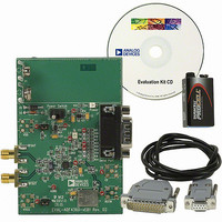
Kit Contents
Board
Main Purpose
Timing, Frequency Synthesizer
Embedded
No
Utilized Ic / Part
ADF4360-7
Primary Attributes
Single Integer-N PLL with VCO
Secondary Attributes
900MHz, 200kHz PFD
Frequency
1.8GHz
Rohs Compliant
Yes
Lead Free Status / RoHS Status
Lead free / RoHS Compliant
Other names
EVAL-ADF4360-7EB1
EVAL-ADF4360-7EB1
Q5173330
Q5652985
EVAL-ADF4360-7EB1
Q5173330
Q5652985


ADF4360-7
OUTPUT MATCHING
There are a number of ways to match the output of the
ADF4360-7 for optimum operation; the most basic is to use a
50 Ω resistor to V
nected in series, as shown in Figure 29. Because the resistor is
not frequency dependent, this provides a good broadband
match. The output power in this circuit typically gives
−5 dBm output power into a 50 Ω load.
A better solution is to use a shunt inductor (acting as an RF
choke) to V
output power. Additionally, a series inductor is added after the
dc bypass capacitor to provide a resonant LC circuit. This tunes
the oscillator output and provides approximately 10 dB addi-
tional rejection of the second harmonic. The shunt inductor
needs to be a relatively high value (>40 nH).
Experiments have shown that the circuit shown in Figure 30
provides an excellent match to 50 Ω over a limited operating
range of the ADF4360-7 (850 MHz to 950 MHz). This gives
approximately −2 dBm output power across the specific
frequency range of the ADF4360-7 using 3.9 nH. For other
frequencies, a tuned LC is recommended. Both complementary
architectures can be examined using the EVAL-ADF4360-7EB1
evaluation board.
VCO
Figure 29. Simple ADF4360-7 Output Stage
. This gives a better match and, therefore, more
RF
VCO
V
VCO
OUT
. A dc bypass capacitor of 100 pF is con-
51Ω
100pF
50Ω
Rev. A | Page 24 of 28
If the user does not need the differential outputs available
on the ADF4360-7, the user may either terminate the unused
output or combine both outputs using a balun. The circuit in
Figure 31 shows how best to combine the outputs.
The circuit in Figure 31 is a lumped-lattice-type LC balun. It
is designed for a center frequency of 900 MHz and outputs
5.0 dBm at this frequency. The series 7.5 nH inductor is used to
tune out any parasitic capacitance due to the board layout from
each input, and the remainder of the circuit is used to shift the
output of one RF input by +90° and the second by −90°, thus
combining the two. The action of the 9.0 nH inductor and the
3.3 pF capacitor accomplishes this. The 47 nH is used to provide
an RF choke to feed the supply voltage, and the 100 pF capacitor
provides the necessary dc block. To ensure good RF perform-
ance, the circuits in Figure 30 and Figure 31 are implemented
with Coilcraft 0402/0603 inductors and AVX 0402 thin-film
capacitors.
Alternatively, instead of the LC balun shown in Figure 31, both
outputs may be combined using a 180° rat-race coupler.
Figure 31. Balun for Combining ADF4360-7 RF Outputs
RF
RF
Figure 30. Optimum ADF4360-7 Output Stage
OUT
OUT
A
B
RF
V
VCO
OUT
7.5nH
7.5nH
V
VCO
47nH
3.9pF
9.0nH
3.3pF
9.0nH
3.3pF
7.5nH
47nH
100pF
50Ω
50Ω
Related parts for EVAL-ADF4360-7EBZ1
Image
Part Number
Description
Manufacturer
Datasheet
Request
R

Part Number:
Description:
±1.7g Dual-Axis IMEMS Accelerometer Evaluation Board
Manufacturer:
Analog Devices Inc
Datasheet:

Part Number:
Description:
Inertial Sensor Evaluation System
Manufacturer:
Analog Devices Inc
Datasheet:
Part Number:
Description:
Manufacturer:
Analog Devices Inc
Datasheet:
Part Number:
Description:
Manufacturer:
Analog Devices Inc
Datasheet:
Part Number:
Description:
Manufacturer:
Analog Devices Inc
Datasheet:
Part Number:
Description:
Manufacturer:
Analog Devices Inc
Datasheet:
Part Number:
Description:
Manufacturer:
Analog Devices Inc
Datasheet:
Part Number:
Description:
Manufacturer:
Analog Devices Inc
Datasheet:
Part Number:
Description:
Manufacturer:
Analog Devices Inc
Datasheet:
Part Number:
Description:
Manufacturer:
Analog Devices Inc
Datasheet:
Part Number:
Description:
Manufacturer:
Analog Devices Inc
Datasheet:
Part Number:
Description:
Manufacturer:
Analog Devices Inc
Datasheet:
Part Number:
Description:
Manufacturer:
Analog Devices Inc
Datasheet: