EVAL-ADF4360-7EBZ1 Analog Devices Inc, EVAL-ADF4360-7EBZ1 Datasheet - Page 12
EVAL-ADF4360-7EBZ1
Manufacturer Part Number
EVAL-ADF4360-7EBZ1
Description
PLL/Frequency Synthesizer EVAL BOARD
Manufacturer
Analog Devices Inc
Datasheet
1.ADF4360-7BCPZ.pdf
(28 pages)
Specifications of EVAL-ADF4360-7EBZ1
Silicon Manufacturer
Analog Devices
Application Sub Type
Integer-N Synthesizer
Kit Application Type
Clock & Timing
Silicon Core Number
ADF4360-7
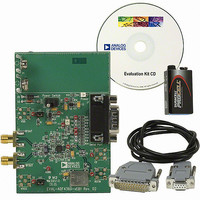
Kit Contents
Board
Main Purpose
Timing, Frequency Synthesizer
Embedded
No
Utilized Ic / Part
ADF4360-7
Primary Attributes
Single Integer-N PLL with VCO
Secondary Attributes
900MHz, 200kHz PFD
Frequency
1.8GHz
Rohs Compliant
Yes
Lead Free Status / RoHS Status
Lead free / RoHS Compliant
Other names
EVAL-ADF4360-7EB1
EVAL-ADF4360-7EB1
Q5173330
Q5652985
EVAL-ADF4360-7EB1
Q5173330
Q5652985


ADF4360-7
After band selection, normal PLL action resumes. The
value of K
(see the Choosing the Correct Inductance section). If divide-by-
2 operation has been selected (by programming DIV2 [DB22]
high in the N counter latch), the value is halved. The ADF4360
family contains linearization circuitry to minimize any variation
of the product of I
The operating current in the VCO core is programmable in four
steps: 5 mA, 10 mA, 15 mA, and 20 mA. This is controlled by
Bits PC1 and PC2 in the control latch.
OUTPUT STAGE
The RF
nected to the collectors of an NPN differential pair driven by
buffered outputs of the VCO, as shown in Figure 21. To allow
the user to optimize the power dissipation vs. the output power
requirements, the tail current of the differential pair is pro-
grammable via Bits PL1 and PL2 in the control latch. Four cur-
rent levels may be set: 3.5 mA, 5 mA, 7.5 mA, and 11 mA. These
levels give output power levels of −14 dBm, −11 dBm, −8 dBm,
and −5 dBm, respectively, using a 50 Ω resistor to V
coupling into a 50 Ω load. Alternatively, both outputs can be
combined in a 1 + 1:1 transformer or a 180° microstrip coupler
(see the Output Matching section).
OUT
V
A and RF
is determined by the value of inductors used
CP
OUT
and K
B pins of the ADF4360 family are con-
V
.
DD
and ac
Rev. A | Page 12 of 28
If the outputs are used individually, the optimum output stage
consists of a shunt inductor to V
Another feature of the ADF4360 family is that the supply current
to the RF output stage is shut down until the part achieves lock as
measured by the digital lock detect circuitry. This is enabled by the
mute-till-lock detect (MTLD) bit in the control latch.
VCO
Figure 21. Output Stage ADF4360-7
DIVIDE BY 2
BUFFER/
DD
RF
.
OUT
A
RF
OUT
B
Related parts for EVAL-ADF4360-7EBZ1
Image
Part Number
Description
Manufacturer
Datasheet
Request
R

Part Number:
Description:
±1.7g Dual-Axis IMEMS Accelerometer Evaluation Board
Manufacturer:
Analog Devices Inc
Datasheet:

Part Number:
Description:
Inertial Sensor Evaluation System
Manufacturer:
Analog Devices Inc
Datasheet:
Part Number:
Description:
Manufacturer:
Analog Devices Inc
Datasheet:
Part Number:
Description:
Manufacturer:
Analog Devices Inc
Datasheet:
Part Number:
Description:
Manufacturer:
Analog Devices Inc
Datasheet:
Part Number:
Description:
Manufacturer:
Analog Devices Inc
Datasheet:
Part Number:
Description:
Manufacturer:
Analog Devices Inc
Datasheet:
Part Number:
Description:
Manufacturer:
Analog Devices Inc
Datasheet:
Part Number:
Description:
Manufacturer:
Analog Devices Inc
Datasheet:
Part Number:
Description:
Manufacturer:
Analog Devices Inc
Datasheet:
Part Number:
Description:
Manufacturer:
Analog Devices Inc
Datasheet:
Part Number:
Description:
Manufacturer:
Analog Devices Inc
Datasheet:
Part Number:
Description:
Manufacturer:
Analog Devices Inc
Datasheet: