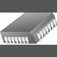
CS5102A-BL Cirrus Logic Inc, CS5102A-BL Datasheet - Page 32

CS5102A-BL
Manufacturer Part Number
CS5102A-BL
Description
A/D Converter (A-D) IC
Manufacturer
Cirrus Logic Inc
Specifications of CS5102A-BL
Input Channels Per Adc
2
Mounting Type
Surface Mount
No. Of Channels
2
Power Rating
44mW
Supply Voltage Min
4.5V
Peak Reflow Compatible (260 C)
No
Sample Rate
20kSPS
Supply Voltage Max
5.5V
Lead Free Status / RoHS Status
Contains lead / RoHS non-compliant
Available stocks
Company
Part Number
Manufacturer
Quantity
Price
Part Number:
CS5102A-BL
Manufacturer:
CRYSTAL
Quantity:
20 000
Company:
Part Number:
CS5102A-BLZ
Manufacturer:
Cirrus Logic Inc
Quantity:
10 000
Part Number:
CS5102A-BLZ
Manufacturer:
CRYSTAL
Quantity:
20 000
Power Supply Connections
VD+ - Positive Digital Power, PIN 7.
VD- - Negative Digital Power, PIN 1.
DGND - Digital Ground, PIN 6.
VA+ - Positive Analog Power, PIN 25.
VA- - Negative Analog Power, PIN 23.
AGND - Analog Ground, PIN 22.
Oscillator
CLKIN - Clock Input, PIN 3.
XOUT - Crystal Output, PIN 4.
Digital Inputs
HOLD - Hold, PIN 12.
CRS/FIN - Coarse Charge/Fine Charge Control, PIN 10.
32
Positive digital power supply. Nominally +5 volts.
Negative digital power supply. Nominally -5 volts.
Digital ground [reference].
Positive analog power supply. Nominally +5 volts.
Negative analog power supply. Nominally -5 volts.
Analog ground reference.
All conversions and calibrations are timed from a master clock which can be externally
supplied by driving CLKIN [this input TTL-compatible, CMOS recommended].
The master clock can be generated by tying a crystal across the CLKIN and XOUT pins. If an
external clock is used, XOUT must be left floating.
A falling transition on this pin sets the CS5101A or CS5102A to the hold state and initiates a
conversion. This input must remain low for at least 1/tclk + 20 ns. When operating in Free Run
Mode, HOLD is disabled, and should be tied to DGND or VD+.
When brought high during acquisition time, CRS/FIN forces the CS5101A or CS5102A into
coarse charge state. This engages the internal buffer amplifier to track the analog input and
charges the capacitor array much faster, thereby allowing the CS5101A or CS5102A to track
high slewing signals. In order to get an accurate sample, the last coarse charge period before
initiating a conversion (bringing HOLD low) must be longer than 0.75
3.75 s (CS5102A). Similarly, the fine charge period immediately prior to conversion must be
at least 1.125 s (CS5101A) or 5.625 s (CS5102A). The CRS/FIN pin must be low during
conversion time. For normal operation, CRS/FIN should be tied low, in which case the
CS5101A or CS5102A will automatically enter coarse charge for 6 clock cycles immediately
after the end of conversion.
CS5101A CS5102A
s (CS5101A) or
DS45F2


