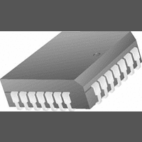
CS5102A-BL Cirrus Logic Inc, CS5102A-BL Datasheet - Page 3

CS5102A-BL
Manufacturer Part Number
CS5102A-BL
Description
A/D Converter (A-D) IC
Manufacturer
Cirrus Logic Inc
Specifications of CS5102A-BL
Input Channels Per Adc
2
Mounting Type
Surface Mount
No. Of Channels
2
Power Rating
44mW
Supply Voltage Min
4.5V
Peak Reflow Compatible (260 C)
No
Sample Rate
20kSPS
Supply Voltage Max
5.5V
Lead Free Status / RoHS Status
Contains lead / RoHS non-compliant
Available stocks
Company
Part Number
Manufacturer
Quantity
Price
Part Number:
CS5102A-BL
Manufacturer:
CRYSTAL
Quantity:
20 000
Company:
Part Number:
CS5102A-BLZ
Manufacturer:
Cirrus Logic Inc
Quantity:
10 000
Part Number:
CS5102A-BLZ
Manufacturer:
CRYSTAL
Quantity:
20 000
ANALOG CHARACTERISTICS
Notes: 6. Applies only in the track mode. When converting or calibrating, input capacitance will not exceed 30 pF.
DS45F2
Specified Temperature Range
Analog Input
Aperture Time
Aperture Jitter
Input Capacitance
Conversion & Throughput
Conversion Time
Acquisition Time
Throughput
Power Supplies
Power Supply Current
(SLEEP High)
Power Consumption
Power Supply Rejection:
10. All outputs unloaded. All inputs at VD+ or DGND.
11. Power consumption in the sleep mode applies with no master clock applied (CLKIN held high or low).
12. With 300 mV p-p, 1 kHz ripple applied to each supply separately in the bipolar mode. Rejection
7. Conversion time scales directly to the master clock speed. The times shown are for synchronous,
8. The CS5101A requires 6 clock cycles of coarse charge, followed by a minimum of 1.125 s of fine charge.
9. Throughput is the sum of the acquisition and conversion times. It will vary in accordance with conditions
internal loopback (FRN mode) with 8.0 MHz CLKIN. In PDT, RBT, and SSC modes, asynchronous delay
between the falling edge of HOLD and the start of conversion may add to the apparent conversion time.
This delay will not exceed 1.5 master clock cycles + 10 ns. In PDT, RBT, and SSC modes, CLKIN can
be increased as long as the HOLD sample rate is 100 kHz max.
FRN mode allows 9 clock cycles for fine charge which provides for the minimum 1.125 s with an 8 MHz
clock, however; in PDT, RBT, or SSC modes, at clock frequencies of 8 MHz or less, fine charge may
be less than 9 clock cycles. This reflects the typ. specification (6 clock cycles + 1.125 s).
affecting acquisition and conversion times, as described above.
improves by 6 dB in the unipolar mode to 90 dB. Figure 23 shows a plot of typical power supply
rejection versus frequency.
Parameter*
Unipolar Mode
Bipolar Mode
Positive Analog
Negative Analog
Positive Digital
Negative Digital
(SLEEP High)
(SLEEP Low)
Negative Supplies
Positive Supplies
(Notes 10, 11)
(Note 10)
(Note 12)
(Note 7)
(Note 8)
(Note 9)
(Note 6)
-16
-16
-16
-8
-8
-8
Symbol Min Typ Max Min Typ Max
PSR
PSR
P
I
P
I
I
I
f
f
D
A
t
tc
t
ta
D
A
-
-
-
-
-
tp
tp
a
do
ds
c
(continued)
+
+
-
-
100
CS5101A -J,K
50
-
-
-
-
-
-
-
-
-
-
-
-
-
-
-
-
0 to +70
100
320
200
320
-21
-11
2.6
25
21
11
84
84
1
-
-
-
-
-
16.25
8.12
1.88
3.75
425
265
430
-28
-15
28
15
-
-
-
-
-
-
-
100
CS5101A -A,B
50
-
-
-
-
-
-
-
-
-
-
-
-
-
-
-
-
40 to +85
100
320
200
320
-21
-11
2.6
25
21
11
84
84
1
-
-
-
-
-
16.25
8.12
1.88
3.75
425
265
430
-28
-15
28
15
-
-
-
-
-
-
-
CS5101A
Units
mW
mW
kHz
kHz
ps
mA
mA
mA
mA
dB
dB
pF
pF
ns
C
s
s
s
s
3


