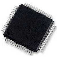
P89LPC9401FBD NXP Semiconductors, P89LPC9401FBD Datasheet - Page 8

P89LPC9401FBD
Manufacturer Part Number
P89LPC9401FBD
Description
IC, MCU 8BIT 80C51, LCD DRIVER, SMD
Manufacturer
NXP Semiconductors
Datasheet
1.P89LPC9401FBD551.pdf
(59 pages)
Specifications of P89LPC9401FBD
Controller Family/series
(8051) 8052
Core Size
8bit
No. Of I/o's
23
Program Memory Size
8KB
Ram Memory Size
256Byte
Cpu Speed
18MHz
Oscillator Type
External, Internal
No. Of Timers
4
No.
RoHS Compliant
Available stocks
Company
Part Number
Manufacturer
Quantity
Price
Part Number:
P89LPC9401FBD
Manufacturer:
NXP/恩智浦
Quantity:
20 000
Company:
Part Number:
P89LPC9401FBD,551
Manufacturer:
NXP Semiconductors
Quantity:
10 000
Company:
Part Number:
P89LPC9401FBD,557
Manufacturer:
NXP Semiconductors
Quantity:
10 000
Company:
Part Number:
P89LPC9401FBDЈ¬551
Manufacturer:
NXP
Quantity:
3 048
Philips Semiconductors
Table 3:
P89LPC9401_1
Preliminary data sheet
Symbol
P0.1/CIN2B/
KBI1
P0.2/CIN2A/
KBI2
P0.3/CIN1B/
KBI3
P0.4/ CIN1A/
KBI4
P0.5/
CMPREF/
KBI5
P0.6/CMP1/
KBI6
P0.7/T1/KBI7
P1.0 to P1.7
P1.0/TXD
P1.1/RXD
P1.2/T0/SCL
P1.3/INTO/
SDA
P1.4/INT1
Pin description
Pin
5
4
3
2
1
24
23
22
21
17
16
15
…continued
Type Description
I/O
I
I
I/O
I
I
I/O
I
I
I/O
I
I
I/O
I
I
I/O
O
I
I/O
I/O
I
I/O, I
I/O
O
I/O
I
I/O
I/O
I/O
I/O
I
I/O
I
I
[1]
P0.6 — Port 0 bit 6.
CMP1 — Comparator 1 output.
KBI6 — Keyboard input 6.
P0.7 — Port 0 bit 7.
T1 — Timer/counter 1 external count input or overflow output.
KBI7 — Keyboard input 7.
P0.1 — Port 0 bit 1.
CIN2B — Comparator 2 positive input B.
KBI1 — Keyboard input 1.
P0.2 — Port 0 bit 2.
CIN2A — Comparator 2 positive input A.
KBI2 — Keyboard input 2.
P0.3 — Port 0 bit 3.
CIN1B — Comparator 1 positive input B.
KBI3 — Keyboard input 3.
P0.4 — Port 0 bit 4.
CIN1A — Comparator 1 positive input A.
KBI4 — Keyboard input 4.
P0.5 — Port 0 bit 5.
CMPREF — Comparator reference (negative) input.
KBI5 — Keyboard input 5.
Port 1: Port 1 is an 8-bit I/O port with a user-configurable output type, except for three
pins as noted below. During reset Port 1 latches are configured in the input only mode
with the internal pull-up disabled. The operation of the configurable Port 1 pins as
inputs and outputs depends upon the port configuration selected. Each of the
configurable port pins are programmed independently. Refer to
configurations”
are open drain when used as outputs. P1.5 is input only.
All pins have Schmitt trigger inputs.
Port 1 also provides various special functions as described below:
P1.0 — Port 1 bit 0.
TXD — Transmitter output for the serial port.
P1.1 — Port 1 bit 1.
RXD — Receiver input for the serial port.
P1.2 — Port 1 bit 2 (open-drain when used as output).
T0 — Timer/counter 0 external count input or overflow output (open-drain when used
as output).
SCL — I
P1.3 — Port 1 bit 3 (open-drain when used as output).
INT0 — External interrupt 0 input.
SDA — I
P1.4 — Port 1 bit 4.
INT1 — External interrupt 1 input.
8-bit two-clock 80C51 microcontroller with 32 segment
2
2
C-bus serial clock input/output.
C-bus serial data input/output.
Rev. 01 — 5 September 2005
and
Table 11 “Static electrical characteristics”
© Koninklijke Philips Electronics N.V. 2005. All rights reserved.
P89LPC9401
for details. P1.2 and P1.3
Section 7.13.1 “Port
4 LCD driver
8 of 59


