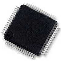
P89LPC9401FBD NXP Semiconductors, P89LPC9401FBD Datasheet - Page 48

P89LPC9401FBD
Manufacturer Part Number
P89LPC9401FBD
Description
IC, MCU 8BIT 80C51, LCD DRIVER, SMD
Manufacturer
NXP Semiconductors
Datasheet
1.P89LPC9401FBD551.pdf
(59 pages)
Specifications of P89LPC9401FBD
Controller Family/series
(8051) 8052
Core Size
8bit
No. Of I/o's
23
Program Memory Size
8KB
Ram Memory Size
256Byte
Cpu Speed
18MHz
Oscillator Type
External, Internal
No. Of Timers
4
No.
RoHS Compliant
Available stocks
Company
Part Number
Manufacturer
Quantity
Price
Part Number:
P89LPC9401FBD
Manufacturer:
NXP/恩智浦
Quantity:
20 000
Company:
Part Number:
P89LPC9401FBD,551
Manufacturer:
NXP Semiconductors
Quantity:
10 000
Company:
Part Number:
P89LPC9401FBD,557
Manufacturer:
NXP Semiconductors
Quantity:
10 000
Company:
Part Number:
P89LPC9401FBDЈ¬551
Manufacturer:
NXP
Quantity:
3 048
Philips Semiconductors
Table 13:
V
T
P89LPC9401_1
Preliminary data sheet
Symbol
f
f
f
T
f
Glitch filter
t
t
External clock
t
t
t
t
Shift register (UART mode 0)
T
t
t
t
t
SPI interface
f
T
t
t
osc(RC)
osc(WD)
osc
CLKLP
gr
sa
CHCX
CLCX
CLCH
CHCL
QVXH
XHQX
XHDX
XHDV
SPI
SPILEAD
SPILAG
amb
DD
cy(CLK)
XLXL
SPICYC
= 3.0 V to 3.6 V unless otherwise specified.
= 40 C to +85 C for industrial applications, unless otherwise specified.
Dynamic characteristics (18 MHz)
Parameter
internal RC oscillator frequency
internal watchdog oscillator frequency
oscillator frequency
clock cycle time
active frequency on pin CLKLP
glitch rejection time
signal acceptance
clock HIGH time
clock LOW time
clock rise time
clock fall time
serial port clock cycle time
output data set-up to clock rising edge
time
output data hold after clock rising
edge time
input data hold after clock rising edge
time
input data valid to clock rising edge
time
SPI operating frequency
SPI cycle time
SPI enable lead time (slave)
SPI enable lag time (slave)
slave
master
slave
master
8-bit two-clock 80C51 microcontroller with 32 segment
Rev. 01 — 5 September 2005
Conditions
see
P1.5/RST pin
any pin except
P1.5/RST
P1.5/RST pin
any pin except
P1.5/RST
see
see
see
see
see
see
see
see
see
see
20, 21,
see
22
see
22
Figure 18
Figure 18
Figure 18
Figure 18
Figure 18
Figure 17
Figure 17
Figure 17
Figure 17
Figure 17
Figure
Figure
Figure
22
19,
21,
21,
16T
13T
7.189
6
4
Min
320
125
150
250
250
CCLK
CCLK
55
50
22
22
cy(CLK)
cy(CLK)
0
0
0
-
-
-
-
-
-
-
Variable clock
[1] [2]
T
T
cy(CLK)
T
cy(CLK)
cy(CLK)
7.557
CCLK
CCLK
Max
520
© Koninklijke Philips Electronics N.V. 2005. All rights reserved.
18
50
15
8
5
5
0
-
-
-
-
-
-
-
-
-
-
+ 20
6
4
t
t
P89LPC9401
CHCX
CLCX
f
7.189
osc
Min
320
125
888
722
150
333
222
250
250
50
22
22
0
-
-
-
-
-
-
-
-
-
-
= 18 MHz
4 LCD driver
7.557 MHz
Max
520
3.0
4.5
50
15
75
5
5
0
-
-
-
-
-
-
-
-
-
-
-
-
-
-
48 of 59
Unit
kHz
MHz
ns
MHz
ns
ns
ns
ns
ns
ns
ns
ns
ns
ns
ns
ns
ns
MHz
MHz
ns
ns
ns
ns


