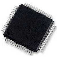
P89LPC9401FBD NXP Semiconductors, P89LPC9401FBD Datasheet - Page 39

P89LPC9401FBD
Manufacturer Part Number
P89LPC9401FBD
Description
IC, MCU 8BIT 80C51, LCD DRIVER, SMD
Manufacturer
NXP Semiconductors
Datasheet
1.P89LPC9401FBD551.pdf
(59 pages)
Specifications of P89LPC9401FBD
Controller Family/series
(8051) 8052
Core Size
8bit
No. Of I/o's
23
Program Memory Size
8KB
Ram Memory Size
256Byte
Cpu Speed
18MHz
Oscillator Type
External, Internal
No. Of Timers
4
No.
RoHS Compliant
Available stocks
Company
Part Number
Manufacturer
Quantity
Price
Part Number:
P89LPC9401FBD
Manufacturer:
NXP/恩智浦
Quantity:
20 000
Company:
Part Number:
P89LPC9401FBD,551
Manufacturer:
NXP Semiconductors
Quantity:
10 000
Company:
Part Number:
P89LPC9401FBD,557
Manufacturer:
NXP Semiconductors
Quantity:
10 000
Company:
Part Number:
P89LPC9401FBDЈ¬551
Manufacturer:
NXP
Quantity:
3 048
Philips Semiconductors
P89LPC9401_1
Preliminary data sheet
7.26.13.1 I
7.26.11 Output bank selector
7.26.12 Input bank selector
7.26.13 Blinker
7.26.14 Input filters
The LCD controller includes a RAM bank switching feature in the static and 1:2 drive
modes. In the static drive mode, the BANK SELECT command may request the contents
of bit 2 to be selected for display instead of the contents of bit 0. In 1:2 mode, the contents
of bits 2 and 3 may be selected instead of bits 0 and 1. This allows display information to
be prepared in an alternative bank and then selected for display when it is assembled.
The input bank selector loads display data into the display RAM based on the selected
LCD drive configuration. The BANK SELECT command can be used to load display data
in bit 2 in static drive mode or in bits 2 and 3 in 1:2 mode. The input bank selector
functions are independent of the output bank selector.
The LCD controller has a very versatile display blinking capability. The whole display can
blink at a frequency selected by the BLINK command. Each blink frequency is a multiple
integer value of the clock frequency; the ratio between the clock frequency and blink
frequency depends on the blink mode selected, as shown in
An additional feature allows an arbitrary selection of LCD segments to be blinked in the
static and 1 : 2 drive modes. This is implemented without any communication overheads
by the output bank selector which alternates the displayed data between the data in the
display RAM bank and the data in an alternative RAM bank at the blink frequency. This
mode can also be implemented by the BLINK command.
The entire display can be blinked at a frequency other than the nominal blink frequency by
sequentially resetting and setting the display enable bit E at the required rate using the
MODE SET command.
Table 8:
Blink modes 0.5 Hz, 1 Hz and 2 Hz, and nominal blink frequencies 0.5 Hz, 1 Hz and 2 Hz
correspond to an oscillator frequency (f
frequency range is 397 Hz to 3046 Hz.
The LCD controller acts as an I
subaddress inputs A0, A,1 and A2 are tied to V
To enhance noise immunity in electrically adverse environments, RC low-pass filters are
provided on the SDA and SCL lines.
Blink mode
Off
2 Hz
1 Hz
0.5 Hz
2
C-bus controller
Blinking frequencies
8-bit two-clock 80C51 microcontroller with 32 segment
Rev. 01 — 5 September 2005
Normal operating mode ratio Normal blink frequency
-
f
f
f
osc(LCD)
osc(LCD)
osc(LCD)
2
C-bus slave receiver. In the P89LPC9401 the hardware
/ 768
/ 1536
/ 3072
osc(LCD)
) of 1536 Hz at pin CLK. The oscillator
SS
setting the hardware subaddress = 0.
© Koninklijke Philips Electronics N.V. 2005. All rights reserved.
Blinking off
2 Hz
1 Hz
0.5 Hz
Table
P89LPC9401
8.
4 LCD driver
39 of 59


