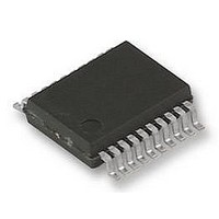
UPD78F9222MC(T)-5A4-A NEC, UPD78F9222MC(T)-5A4-A Datasheet - Page 60

UPD78F9222MC(T)-5A4-A
Manufacturer Part Number
UPD78F9222MC(T)-5A4-A
Description
8BIT MCU, 4K FLASH, 256B RAM, 78F9222
Manufacturer
NEC
Datasheet
1.UPD78F9222MCT-5A4-A.pdf
(414 pages)
Specifications of UPD78F9222MC(T)-5A4-A
Controller Family/series
UPD78
No. Of I/o's
17
Ram Memory Size
256Byte
Cpu Speed
10MHz
No. Of Timers
4
No. Of
RoHS Compliant
Core Size
8bit
Program Memory Size
4KB
Oscillator Type
External, Internal
Available stocks
Company
Part Number
Manufacturer
Quantity
Price
Company:
Part Number:
UPD78F9222MC(T)-5A4-A
Manufacturer:
NEC
Quantity:
1 000
Company:
Part Number:
UPD78F9222MC(T)-5A4-A
Manufacturer:
NEC/PBF
Quantity:
6 640
Part Number:
UPD78F9222MC(T)-5A4-A
Manufacturer:
RENESAS/瑞萨
Quantity:
20 000
- Current page: 60 of 414
- Download datasheet (4Mb)
4.2.4
port mode register 12 (PM12). When the P123 pin is used as an input port, an on-chip pull-up resistor can be
connected by using pull-up resistor option register 12 (PU12).
P121 and P122 pins differ, therefore, depending on the selected system clock oscillator. The following three system
clock oscillators can be used.
(1) High-speed internal oscillator
(2) Crystal/ceramic oscillator
(3) External clock input
60
Port 12 is a 3-bit I/O port with an output latch. Each bit of this port can be set to the input or output mode by using
The P121 and P122 pins are also used as the X1 and X2 pins of the system clock oscillator. The functions of the
The system clock oscillation is selected by the option byte. For details, refer to CHAPTER 17 OPTION BYTE.
Reset signal generation sets port 12 to the input mode.
Figures 4-10 and 4-11 show the block diagrams of port 12.
The P121 and P122 pins can be used as I/O port pins.
The P121 and P122 pins cannot be used as I/O port pins because they are used as the X1 and X2 pins.
The P121 pin is used as the X1 pin to input an external clock, and therefore it cannot be used as an I/O port pin.
The P122 pin can be used as an I/O port pin.
Port 12
P12:
PM12:
RD:
WR××: Write signal
WR
WR
RD
Port register 12
Port mode register 12
Read signal
PORT
PM
PM121, PM122
(P121, P122)
Output latch
Figure 4-10. Block Diagram of P121 and P122
PM12
P12
CHAPTER 4 PORT FUNCTIONS
User’s Manual U16898EJ5V0UD
P121/X1,
P122/X2
Related parts for UPD78F9222MC(T)-5A4-A
Image
Part Number
Description
Manufacturer
Datasheet
Request
R

Part Number:
Description:
16/8 bit single-chip microcomputer
Manufacturer:
NEC
Datasheet:

Part Number:
Description:
Dual audio power amp circuit
Manufacturer:
NEC
Datasheet:

Part Number:
Description:
Dual comparator
Manufacturer:
NEC
Datasheet:

Part Number:
Description:
MOS type composite field effect transistor
Manufacturer:
NEC
Datasheet:

Part Number:
Description:
50 V/100 mA FET array incorporating 2 N-ch MOSFETs
Manufacturer:
NEC
Datasheet:

Part Number:
Description:
6-pin small MM high-frequency double transistor
Manufacturer:
NEC
Datasheet:

Part Number:
Description:
6-pin small MM high-frequency double transistor
Manufacturer:
NEC
Datasheet:

Part Number:
Description:
6-pin small MM high-frequency double transistor
Manufacturer:
NEC
Datasheet:

Part Number:
Description:
6-pin small MM high-frequency double transistor
Manufacturer:
NEC
Datasheet:

Part Number:
Description:
Twin transistors equipped with different model chips(6P small MM)
Manufacturer:
NEC
Datasheet:

Part Number:
Description:
Bipolar analog integrated circuit
Manufacturer:
NEC
Datasheet:


