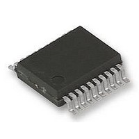
UPD78F9222MC(T)-5A4-A NEC, UPD78F9222MC(T)-5A4-A Datasheet - Page 392

UPD78F9222MC(T)-5A4-A
Manufacturer Part Number
UPD78F9222MC(T)-5A4-A
Description
8BIT MCU, 4K FLASH, 256B RAM, 78F9222
Manufacturer
NEC
Datasheet
1.UPD78F9222MCT-5A4-A.pdf
(414 pages)
Specifications of UPD78F9222MC(T)-5A4-A
Controller Family/series
UPD78
No. Of I/o's
17
Ram Memory Size
256Byte
Cpu Speed
10MHz
No. Of Timers
4
No. Of
RoHS Compliant
Core Size
8bit
Program Memory Size
4KB
Oscillator Type
External, Internal
Available stocks
Company
Part Number
Manufacturer
Quantity
Price
Company:
Part Number:
UPD78F9222MC(T)-5A4-A
Manufacturer:
NEC
Quantity:
1 000
Company:
Part Number:
UPD78F9222MC(T)-5A4-A
Manufacturer:
NEC/PBF
Quantity:
6 640
Part Number:
UPD78F9222MC(T)-5A4-A
Manufacturer:
RENESAS/瑞萨
Quantity:
20 000
- Current page: 392 of 414
- Download datasheet (4Mb)
392
A/D
converter
Function
Input range of
ANI0 to ANI3
Conflicting
operations
Noise counter-
measures
ANI0/P20 to
ANI3/P23
Input
impedance of
ANI0 to ANI3
pins
Details of
Function
Observe the rated range of the ANI0 to ANI3 input voltage. If a voltage of AV
or higher and V
input to an analog input channel, the converted value of that channel becomes
undefined. In addition, the converted values of the other channels may also be
affected.
Conflict between A/D conversion result register (ADCR, ADCRH) write and
ADCR, ADCRH read by instruction upon the end of conversion ADCR, ADCRH
read has priority. After the read operation, the new conversion result is written
to ADCR, ADCRH.
Conflict between ADCR, ADCRH write and A/D converter mode register (ADM)
write or analog input channel specification register (ADS) write upon the end of
conversion ADM or ADS write has priority. ADCR, ADCRH write is not
performed, nor is the conversion end interrupt signal (INTAD) generated.
To maintain the 10-bit resolution, attention must be paid to noise input to the
AV
<1> Connect a capacitor with a low equivalent resistance and a high frequency
<2> Because the effect increases in proportion to the output impedance of the
<3> Do not switch the A/D conversion function of the ANI0 to ANI3 pins to their
<4> The conversion accuracy can be improved by setting HALT mode
The analog input pins (ANI0 to ANI3) are also used as I/O port pins (P20 to
P23).
When A/D conversion is performed with any of ANI0 to ANI3 selected, do not
access P20 to P23 while conversion is in progress; otherwise the conversion
resolution may be degraded.
If a digital pulse is applied to the pins adjacent to the pins currently used for A/D
conversion, the expected value of the A/D conversion may not be obtained due
to coupling noise. Therefore, do not apply a pulse to the pins adjacent to the
pin undergoing A/D conversion.
In this A/D converter, the internal sampling capacitor is charged and sampling is
performed during sampling time.
Since only the leakage current flows other than during sampling and the current
for charging the capacitor also flows during sampling, the input impedance
fluctuates both during sampling and otherwise.
If the shortest conversion time of the reference voltage is used, to perform
sufficient sampling, it is recommended to make the output impedance of the
analog input source 1 kΩ or lower, or attach a capacitor of around 0.01
0.1
REF
µ
analog input source, it is recommended that a capacitor be connected
externally, as shown in Figure 9-19, to reduce noise.
alternate functions during conversion.
immediately after the conversion starts.
response to the power supply.
F to the ANI0 to ANI3 pins (see Figure 10-19).
pin and ANI0 to ANI3 pins.
APPENDIX D LIST OF CAUTIONS
User’s Manual U16898EJ5V0UD
SS
or lower (even in the range of absolute maximum ratings) is
Cautions
µ
F to
REF
p. 175
p. 175
p. 175
p. 176
p. 176
p. 176
p. 176
Page
(9/19)
Related parts for UPD78F9222MC(T)-5A4-A
Image
Part Number
Description
Manufacturer
Datasheet
Request
R

Part Number:
Description:
16/8 bit single-chip microcomputer
Manufacturer:
NEC
Datasheet:

Part Number:
Description:
Dual audio power amp circuit
Manufacturer:
NEC
Datasheet:

Part Number:
Description:
Dual comparator
Manufacturer:
NEC
Datasheet:

Part Number:
Description:
MOS type composite field effect transistor
Manufacturer:
NEC
Datasheet:

Part Number:
Description:
50 V/100 mA FET array incorporating 2 N-ch MOSFETs
Manufacturer:
NEC
Datasheet:

Part Number:
Description:
6-pin small MM high-frequency double transistor
Manufacturer:
NEC
Datasheet:

Part Number:
Description:
6-pin small MM high-frequency double transistor
Manufacturer:
NEC
Datasheet:

Part Number:
Description:
6-pin small MM high-frequency double transistor
Manufacturer:
NEC
Datasheet:

Part Number:
Description:
6-pin small MM high-frequency double transistor
Manufacturer:
NEC
Datasheet:

Part Number:
Description:
Twin transistors equipped with different model chips(6P small MM)
Manufacturer:
NEC
Datasheet:

Part Number:
Description:
Bipolar analog integrated circuit
Manufacturer:
NEC
Datasheet:


