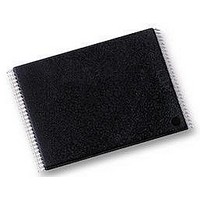
H27UF081G1M-TPCB HYNIX SEMICONDUCTOR, H27UF081G1M-TPCB Datasheet - Page 12

H27UF081G1M-TPCB
Manufacturer Part Number
H27UF081G1M-TPCB
Description
IC, MEMORY, FLASH NAND 1GB, TSOP48
Manufacturer
HYNIX SEMICONDUCTOR
Datasheet
1.H27UF081G1M-TPCB.pdf
(39 pages)
Specifications of H27UF081G1M-TPCB
Access Time
45ns
Supply Voltage Range
2.7V To 3.6V
Memory Case Style
TSOP
No. Of Pins
48
Operating Temperature Range
0°C To +70°C
Base Number
27
Interface
Serial
Logic
RoHS Compliant
Package / Case
TSOP
Memory Type
Flash - NAND
Memory Configuration
128M X 8
Rohs Compliant
Yes
Memory Size
1Gbit
3.3 Block Erase.
The Erase operation is done on a block (16K Byte) basis. It consists of an Erase Setup command (60h), a Block address
loading and an Erase Confirm Command (D0h). The Erase Confirm command (D0h) following the block address loading
initiates the internal erasing process. This two-step sequence of setup followed by execution command ensures that
memory contents are not accidentally erased due to external noise conditions.
The block address loading is accomplished in four cycles depending on the device density. Only block addresses (A14 to
A26) are needed while A9 to A13 is ignored. At the rising edge of WE after the erase confirm command input, the inter-
nal Program Erase Controller handles erase and erase-verify. When the erase operation is completed, the Write Status
Bit (I/O 0) may be checked. Figure_16 details the sequence.
3.4 Copy-Back Program.
The copy-back program is provided to quickly and efficiently rewrite data stored in one page within the plane to
another page within the same plane without using an external memory. Since the time-consuming sequential-reading
and its reloading cycles are removed, the system performance is improved. The benefit is especially obvious when a
portion of a block is updated and the rest of the block also need to be copied to the newly assigned free block. The
operation for performing a copy-back program is a sequential execution of page-read without burst-reading cycle and
copying-program with the address of destination page. A normal read operation with "00h" command and the address
of the source page moves the whole 528byte data into the internal buffer. As soon as the device returns to Ready state,
Page-Copy Data-input command (8Ah) with the address cycles of destination page followed may be written. The Pro-
gram Confirm command (10h) is required to actually begin the programming operation.
Copy-Back Program operation is allowed only within the same memory plane. Once the Copy-Back Program is finished,
any additional partial page programming into the copied pages is prohibited before erase. Plane address must be the
same between source and target page
"When there is a program-failure at Copy-Back operation, error is reported by pass/fail status. But, if
Copy-Back operations are accumulated over time, bit error due to charge loss is not checked by external
error detection/correction scheme. For this reason, two bit error correction is recommended for the use
of Copy-Back operation."
Figure 15 shows the command sequence for the copy-back operation.
The Copy Back Program operation requires three steps:
- 1. The source page must be read using the Read A command (one bus write cycle to setup the command and then 3
- 2. When the device returns to the ready state (Ready/Busy High), the second bus write cycle of the command is
- 3. Then the confirm command is issued to start the P/E/R Controller.
Note:
1. Copy-Back Program operation is allowed only within the same memory plane.
2. On the same plane, It’s prohibited to operate copy-back program from an odd address page (source page) to an
Rev 0.2 / May. 2007
even address page (target page) or from an even address page (source page) to an odd address page (target page).
Therefore, the copy-back program is permitted just between odd address pages or even address pages.
bus cycles to input the source page address.) This operation copies all 264 Words/ 528 Bytes from the page into
the page Buffer.
given with the 4cycles to input the target page address. A26, A25 must be the same for the Source and Target
Pages.
1Gbit (128Mx8bit / 64Mx16bit) NAND Flash
HY27US(08/16)1G1M Series
Preliminary
12


