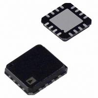
ADXL180WCPZ-RL Analog Devices Inc, ADXL180WCPZ-RL Datasheet - Page 51

ADXL180WCPZ-RL
Manufacturer Part Number
ADXL180WCPZ-RL
Description
IC ACCELEROMETER CONFIG 16-LFCSP
Manufacturer
Analog Devices Inc
Series
iMEMS®r
Datasheet
1.ADXL180WCPZ-RL.pdf
(60 pages)
Specifications of ADXL180WCPZ-RL
Axis
X or Y
Acceleration Range
±50g, 100g, 150g, 200g, 250g, 350g, 500g
Voltage - Supply
5 V ~ 14.5 V
Output Type
Analog
Bandwidth
100Hz ~ 800Hz Selectable
Mounting Type
Surface Mount
Package / Case
16-LFQFN, CSP Exposed Pad
Package Type
LFCSP EP
Operating Supply Voltage (min)
5V
Operating Temperature (min)
-40C
Operating Temperature (max)
125C
Operating Temperature Classification
Automotive
Product Depth (mm)
5mm
Product Height (mm)
1.43mm
Product Length (mm)
5mm
Mounting
Surface Mount
Pin Count
16
Lead Free Status / RoHS Status
Lead free / RoHS Compliant
Sensitivity
-
Interface
-
Lead Free Status / Rohs Status
Compliant
Other names
ADXL180WCPZ-RLCT
The CUPRG bit is automatically programmed to the locked
state (1) at the end of the configuration/user data OTP fuse
programming sequence. This prevents any further writes to the
UREG and CREG RAM registers as well as disables the confi-
guration/user data OTP fuse programming circuitry. The read
value of this bit indicates whether the configuration/user data
OTP memory has been programmed (that is, locked). A 1
indicates that the OTP memory block has been programmed
and further test system writes to either the RAM or OTP
configuration/user data registers are ignored.
OTP PROGRAMMING CONDITIONS AND
CONSIDERATIONS
Note that all configuration/user OTP registers are programmed
when the CUPRG bit is set regardless of whether the registers
have been written to. The OTP registers can be programmed
one time only.
During normal operation and in configuration mode, the
internal voltage regulator is operating at 4.2 V nominal. This
internal voltage changes to a nominal value of 6.5 V during the
time that the ADXL180 is programming the configuration and
user OTP fuses (t
above the minimum fuse programming value specified in the
specification table for proper fuse programming. The V
current is increased during fuse programming as shown in
Figure 41. The configuration/test system must supply at least
the value I
are production tested for user programming at 25°C.
If the minimum programming voltage is not achieved, the
ADXL180 does not respond to subsequent communications
requests because it waits for the required programming voltage.
The device does not attempt to program unless the required
voltage level is achieved. The user’s test system should include
a timeout check if the device does not respond due to this sit-
uation. When properly programmed, the ADXL180 issues a
FP
as specified. The configuration and user registers
CUP
). The V
BP
supply voltage must be held at or
PROGRAM
OTP
FROM RECEIVE
SERIAL PORT
Figure 42. Configuration Mode RAM and OTP Register Structure
FUSE
OTP
BP
supply
CUPRG
DATA
OTP
Rev. A | Page 51 of 60
A
B
SEL
MUX
handshake back to the command module. Do not attempt to
write to the configuration registers or attempt another OTP
programming step until this handshake has been received.
CONFIGURATION/USER REGISTER OTP PARITY
The configuration/user data OTP CU parity bit (CUPAR) must
be programmed to provide even parity for the configuration/
user data OTP memory. The CUPAR bit should be set to either
a 1 or a 0 to make the total number of 1s in the configuration/
user data OTP memory (including the value of the OTP CU
parity bit) an even number. The configuration/user data OTP
memory is defined as CREG0, CREG1, CREG2, and UREG.
The parity calculation must include the state of all register bits
including all of the UD and NU bits. The CUPRG bit must also
be included. During normal operation, once the configuration/
user data programming bit is set, the ADXL180 monitors the
parity of the configuration/user data OTP memory and com-
pares it against the programmed value of the CU parity bit in
CREG2. An OTP parity error is flagged if the monitored parity
and the programmed parity differ. See the Error Detection
section.
CONFIGURATION MODE ERROR REPORTING
The receive communication parity error and the OTP
programming voltage error are the two errors reported by
the ADXL180 when in configuration mode. The OTP parity,
configuration and other normal mode (run-time) errors are
suppressed in configuration mode. The state vector code is set
to a state vector of 5 (101b). The 8-bit error data code is shown
in Table 43. The 4-bit address field is set to 8 (1000b).
Table 43. Configuration Mode Error Codes
0000 0000b
Error Data Code
RAM
TO TRANSMIT
SERIAL PORT AND
CONFIGURATION
CONTROL LOGIC
Configuration mode receive parity error
Error Description
ADXL180


