NUMICRO-SDK Nuvoton Technology Corporation of America, NUMICRO-SDK Datasheet - Page 437
NUMICRO-SDK
Manufacturer Part Number
NUMICRO-SDK
Description
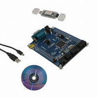
KIT EVAUATION NUC100/120/130/140
Manufacturer
Nuvoton Technology Corporation of America
Series
NuMicro™r
Type
MCUr
Datasheets
1.NUC100LC1BN.pdf
(600 pages)
2.NUMICRO-SDK.pdf
(13 pages)
3.NUMICRO-SDK.pdf
(93 pages)
4.NUMICRO-SDK.pdf
(1 pages)
Specifications of NUMICRO-SDK
Contents
Board, Cable, CD, Nu-Link
Lead Free Status / RoHS Status
Lead free / RoHS Compliant
For Use With/related Products
NUC100, NUC120, NUC130, NUC140
Available stocks
Company
Part Number
Manufacturer
Quantity
Price
Company:

Part Number:
NUMICRO-SDK
Manufacturer:
Nuvoton Technology Corporation
Quantity:
135
Company:
Part Number:
NUMICRO-SDK
Manufacturer:
NuvoTon
Quantity:
69


BUS TIMING Register (BTIMR)
Register
BTIMR
Bits
[31:16]
[15]
[14:11]
[10:6]
[5:4]
[3:0]
Note: According the parameters which defined in the BTIMR, the bit rate clock of CAN can be
calculated as following equation.
SAMP
31
23
15
7
TSEG1[1:0]
NuMicro™ NUC100 Series Technical Reference Manual
Offset
CAN0_BA+0x14
Descriptions
Reserved
SAMP
TSEG2
TSEG1
SJW
Reserved
30
22
14
6
R/W
R/W
Reserved
Number of Sampling Point
1 = Triple; the bus is sampled three times in one bit; they are located in TSEG1 + 1,
TSEG1 and TSEG1 - 1.
Recommended for low/medium speed buses where filtering spikes on the bus line is
beneficial
0 = Single; the bus is sampled once in the location of (TSEG1 + 1); recommended for
high speed buses.
Time Segment 2
(TSEG1 + 1) and (TSEG2 + 1) define the number of clock cycles per bit period and the
location of the sample point.
(TSEG2 +1) defines the sample point location of per bit before the SYNC SEG.
Note: There are three segments including SYNC, TSEG1, and TSEG2 per bit. The
value of TSEG2 is max (TSEG1/2, 2).
Time Segment 1
(TSEG1 + 1) defines the period between the SYNC segment and the sample point (not
including the SYNC segment). The maximum value of TSEG1 is 16 and the minimum
value is 2.
Synchronization Jump Width
To compensate for phase shifts between clock sources of different bus nodes, any
node must re-synchronize on any relevant signal edge of the current transmission. The
SJW defines the maximum number of clock cycles a bit period may be shorted or
lengthened by one re-synchronization. The maximum values of SJW shall be less than
the min{TSEG1, TSEG2}. (see the BTIMR block description)
Reserved
29
21
13
5
TSEG2
Description
Bus Timing Register
SJW
28
20
12
4
- 437 -
Reserved
Reserved
27
19
11
3
Publication Release Date: Oct 22, 2010
26
18
10
2
Reserved
TSEG1[4:2]
25
17
9
1
Revision V1.06
Reset Value
0x0000_1100
24
16
8
0
Related parts for NUMICRO-SDK
Image
Part Number
Description
Manufacturer
Datasheet
Request
R

Part Number:
Description:
IC MCU 32BIT 32KB FLASH 33QFN
Manufacturer:
Nuvoton Technology Corporation of America
Datasheet:
Part Number:
Description:
IC MCU 32BIT 32KB FLASH 48LQFP
Manufacturer:
Nuvoton Technology Corporation of America
Datasheet:

Part Number:
Description:
IC MCU 32BIT 32KB FLASH 48LQFP
Manufacturer:
Nuvoton Technology Corporation of America
Datasheet:

Part Number:
Description:
IC MCU 32BIT 64KB FLASH 33QFN
Manufacturer:
Nuvoton Technology Corporation of America
Datasheet:

Part Number:
Description:
IC MCU 32BIT 32KB FLASH 48LQFP
Manufacturer:
Nuvoton Technology Corporation of America
Datasheet:

Part Number:
Description:
IC MCU 32BIT 64KB FLASH 48LQFP
Manufacturer:
Nuvoton Technology Corporation of America
Datasheet:

Part Number:
Description:
IC MCU 32BIT 64KB FLASH 64LQFP
Manufacturer:
Nuvoton Technology Corporation of America
Datasheet:

Part Number:
Description:
IC MCU 32BIT 64KB FLASH 64LQFP
Manufacturer:
Nuvoton Technology Corporation of America
Datasheet:

Part Number:
Description:
IC MCU 32BIT 64KB FLASH 48LQFP
Manufacturer:
Nuvoton Technology Corporation of America
Datasheet:
Part Number:
Description:
IC MCU 32BIT 64KB FLASH 64LQFP
Manufacturer:
Nuvoton Technology Corporation of America
Datasheet:

Part Number:
Description:
IC MCU 32BIT 8KB FLASH 33QFN
Manufacturer:
Nuvoton Technology Corporation of America
Datasheet:

Part Number:
Description:
IC MCU 32BIT 8KB FLASH 48LQFP
Manufacturer:
Nuvoton Technology Corporation of America
Datasheet:
Part Number:
Description:
IC MCU 32BIT 16KB FLASH 33QFN
Manufacturer:
Nuvoton Technology Corporation of America
Datasheet:
Part Number:
Description:
IC MCU 32BIT 64KB FLASH 100LQFP
Manufacturer:
Nuvoton Technology Corporation of America
Datasheet:

Part Number:
Description:
IC MCU 32BIT 128KB FLASH 64LQFP
Manufacturer:
Nuvoton Technology Corporation of America
Datasheet: