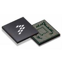
SC900841JVK Freescale Semiconductor, SC900841JVK Datasheet - Page 75

SC900841JVK
Manufacturer Part Number
SC900841JVK
Description
IC POWER MGT 338-MAPBGA
Manufacturer
Freescale Semiconductor
Specifications of SC900841JVK
Applications
PC's, PDA's
Operating Temperature
-40°C ~ 85°C
Mounting Type
Surface Mount
Package / Case
338-TBGA
Input Voltage
2.8 V to 4.4 V
Maximum Operating Temperature
+ 85 C
Minimum Operating Temperature
- 40 C
Lead Free Status / RoHS Status
Lead free / RoHS Compliant
Current - Supply
-
Voltage - Supply
-
Lead Free Status / Rohs Status
Lead free / RoHS Compliant
Available stocks
Company
Part Number
Manufacturer
Quantity
Price
Company:
Part Number:
SC900841JVK
Manufacturer:
Freescale Semiconductor
Quantity:
10 000
Company:
Part Number:
SC900841JVKR2
Manufacturer:
Freescale Semiconductor
Quantity:
10 000
- Current page: 75 of 192
- Download datasheet (8Mb)
Table 34. V21 Status/Control Registers Structure and Bits Description
Efficiency Curves
mode, based on the recommended external component
V21 Status/Control Registers and Bits Description
default state for each of these registers.
V15
Buck PWM voltage-mode control DC/DC regulator.
the load conditions. These modes can be set through the SPI
and include a PFM mode, an Automatic Pulse Skipping
mode, and a PWM mode. The above selection is optimized
to maximum battery life based on load conditions.
down.
AOACCTLV21 5:3
Analog Integrated Circuit Device Data
Freescale Semiconductor
Reserved
The following efficiency curves are calculated under PWM
Reference the register map for read/write conditions and
This is a 4.0 MHz fully integrated 2-switch synchronous
The switcher can operate in different modes depending on
V15 will be discharged every time the regulator is shutting
CTLV21
Name
Bits
2:0
7:6
V21 State Control
x0 = Reserved
x1 = Reserved
x2 = Reserved
x3 = Reserved
V21 State Control during AOAC Exit (when EXITSTBY pin is asserted). These bits will be initialized by the system SPI
controller after power up
X0 = Do not copy
x1 = Do not copy
x2 = Do not copy
x3 = Do not copy
Reserved
V21CNT (ADDR 0x38 - R/W - Default value: 0x07)
Figure 30. V21 Efficiency Waveforms
values and typical output voltage of 2.1 V. 3.0 V ≤ VPW ≤
4.4 V.
ADC, and stored in a register for the processor to access.
protection purposes. If an over-current condition is detected,
the regulator will limit the current through cycle by cycle
operation and alert the system through the V15FAULT signal,
which will in turn assert the VRFAULT Interrupt signal.
automatically set at 1.6 V to maintain voltage headroom for
the operation of 1.3 V VYMXGPS, reference
more details.
Description
The output current is measured internally, digitized by the
The peak current is sensed internally for over-current
Please note that when VYMXGPS is set at 1.3 V, V15 is
x4 = OFF
x5 = PFM
x6 = Automatic Pulse Skipping
x7 = PWM
x4 = OFF
x5 = PFM
x6 = Automatic Pulse Skipping
x7 = PWM
FUNCTIONAL DEVICE OPERATION
POWER SUPPLIES
VYMXGPS
900841
for
75
Related parts for SC900841JVK
Image
Part Number
Description
Manufacturer
Datasheet
Request
R
Part Number:
Description:
Manufacturer:
Freescale Semiconductor, Inc
Datasheet:
Part Number:
Description:
Manufacturer:
Freescale Semiconductor, Inc
Datasheet:
Part Number:
Description:
Manufacturer:
Freescale Semiconductor, Inc
Datasheet:
Part Number:
Description:
Manufacturer:
Freescale Semiconductor, Inc
Datasheet:
Part Number:
Description:
Manufacturer:
Freescale Semiconductor, Inc
Datasheet:
Part Number:
Description:
Manufacturer:
Freescale Semiconductor, Inc
Datasheet:
Part Number:
Description:
Manufacturer:
Freescale Semiconductor, Inc
Datasheet:
Part Number:
Description:
Manufacturer:
Freescale Semiconductor, Inc
Datasheet:
Part Number:
Description:
Manufacturer:
Freescale Semiconductor, Inc
Datasheet:
Part Number:
Description:
Manufacturer:
Freescale Semiconductor, Inc
Datasheet:
Part Number:
Description:
Manufacturer:
Freescale Semiconductor, Inc
Datasheet:
Part Number:
Description:
Manufacturer:
Freescale Semiconductor, Inc
Datasheet:
Part Number:
Description:
Manufacturer:
Freescale Semiconductor, Inc
Datasheet:
Part Number:
Description:
Manufacturer:
Freescale Semiconductor, Inc
Datasheet:
Part Number:
Description:
Manufacturer:
Freescale Semiconductor, Inc
Datasheet:


