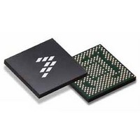
SC900841JVK Freescale Semiconductor, SC900841JVK Datasheet - Page 46

SC900841JVK
Manufacturer Part Number
SC900841JVK
Description
IC POWER MGT 338-MAPBGA
Manufacturer
Freescale Semiconductor
Specifications of SC900841JVK
Applications
PC's, PDA's
Operating Temperature
-40°C ~ 85°C
Mounting Type
Surface Mount
Package / Case
338-TBGA
Input Voltage
2.8 V to 4.4 V
Maximum Operating Temperature
+ 85 C
Minimum Operating Temperature
- 40 C
Lead Free Status / RoHS Status
Lead free / RoHS Compliant
Current - Supply
-
Voltage - Supply
-
Lead Free Status / Rohs Status
Lead free / RoHS Compliant
Available stocks
Company
Part Number
Manufacturer
Quantity
Price
Company:
Part Number:
SC900841JVK
Manufacturer:
Freescale Semiconductor
Quantity:
10 000
Company:
Part Number:
SC900841JVKR2
Manufacturer:
Freescale Semiconductor
Quantity:
10 000
- Current page: 46 of 192
- Download datasheet (8Mb)
SIDEBAND SIGNALS
PMCINT Pin
rising from low to high when an unmasked interrupt event
occurs. It is a level sensitive pin and it is cleared when the
Platform controller hub reads the Interrupt registers.
Reference
explanation of the Interrupt mechanism.
in
VRCOMP Pin
is asserted low by the PMIC when a SPI voltage regulation
request, or other write request has been decoded. The signal
is de-asserted on completion of the request (i.e. the rail is in
regulation). This signal is relevant to the SPI initiated writes
and EXITSTBY assertion.
RESET Pin
hub. When this pin is asserted, the Platform controller hub
returns to its initial default state. This signal can be asserted
46
900841
Table 12. Sidebands Pin Functionality
FUNCTIONAL DEVICE OPERATION
SYSTEM CONTROL INTERFACE
THRMTRIPB
Table 3
The following pins are included as part of the Sideband signals:
The PMICINT pin interrupts the Platform controller hub by
The PMICINT pin follows the DC Signaling specifications
This is an active high voltage regulator complete signal. It
This is an active low, hard reset for the Platform controller
VIDEN[1:0]
EXITSTBY
Pin Name
VRCOMP
PMICINT
RESETB
PWRGD
VID[6:0]
with a reference of 1.8 V (VPMIC).
Interrupt Controller
VR_COMP
VR Status
SPI_CS#
I/O
SPI Bus
O
O
O
O
I
I
I
I
Figure 9. VRCOMP Functionality in a SPI Voltage Regulators Configuration
Active high input signals driven by the CPU, to indicate the output voltage setting for the VCC and VNN rails.
Existing Mode
for a more detailed
Active high Input signals driven by the CPU, to indicate if the VID bus is addressing VCC or VNN.
Idle
SPI Packet SPI Packet SPI Packet SPI Packet
Active low hard reset for Platform controller hub
Active high Voltage Regulator Complete signal
Active low Thermal Trip Assertion Input signal
Active high Power Good Output signal
Active high PMIC Interrupt Output pin
VR Reconfigure
Active high Exit Standby signal
4 - t
VR_COMP
Pin Functionality
in
cycles and VRCOMP functionality. The rising edge on the
SPICSB pin indicates the end of the block of Voltage
Regulators configurations, at which point the VRCOMP pin is
driven low. As an address/data block is written, the PMIC can
start to ramp those rails (DC-DC, LDO, or switch). Once all of
the rails are in regulation, the PMIC drives the VRCOMP pin
high, indicating to the Platform controller hub that the voltage
regulator configuration request is completed, and the PMIC is
ready for subsequent transactions. The maximum number of
voltage regulator change packets (address/data
combinations) is 8. The voltage regulators should ramp at the
rate defined in the regulators tables. Due to the relatively long
turn-off time of the voltage regulators, the VRCOMP signal is
to be gated-off after a 500 ns minimum (30 ms max.) low
time.
when a cold or warm reset is initiated, depending on the
settings in the CHIPCNTL register.
Table 3
Table 3
The VRCOMP pin follows the DC Signaling specifications
Figure 9
The RESET pin follows the DC Signaling specifications in
with a VCC of 1.8 V (VPMIC)
with a reference of 1.8 V (VPMIC).
illustrates the Voltage Regulators register write
Analog Integrated Circuit Device Data
Idle
Freescale Semiconductor
Idle
Related parts for SC900841JVK
Image
Part Number
Description
Manufacturer
Datasheet
Request
R
Part Number:
Description:
Manufacturer:
Freescale Semiconductor, Inc
Datasheet:
Part Number:
Description:
Manufacturer:
Freescale Semiconductor, Inc
Datasheet:
Part Number:
Description:
Manufacturer:
Freescale Semiconductor, Inc
Datasheet:
Part Number:
Description:
Manufacturer:
Freescale Semiconductor, Inc
Datasheet:
Part Number:
Description:
Manufacturer:
Freescale Semiconductor, Inc
Datasheet:
Part Number:
Description:
Manufacturer:
Freescale Semiconductor, Inc
Datasheet:
Part Number:
Description:
Manufacturer:
Freescale Semiconductor, Inc
Datasheet:
Part Number:
Description:
Manufacturer:
Freescale Semiconductor, Inc
Datasheet:
Part Number:
Description:
Manufacturer:
Freescale Semiconductor, Inc
Datasheet:
Part Number:
Description:
Manufacturer:
Freescale Semiconductor, Inc
Datasheet:
Part Number:
Description:
Manufacturer:
Freescale Semiconductor, Inc
Datasheet:
Part Number:
Description:
Manufacturer:
Freescale Semiconductor, Inc
Datasheet:
Part Number:
Description:
Manufacturer:
Freescale Semiconductor, Inc
Datasheet:
Part Number:
Description:
Manufacturer:
Freescale Semiconductor, Inc
Datasheet:
Part Number:
Description:
Manufacturer:
Freescale Semiconductor, Inc
Datasheet:


