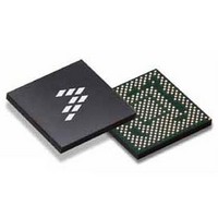
SC900841JVK Freescale Semiconductor, SC900841JVK Datasheet - Page 134

SC900841JVK
Manufacturer Part Number
SC900841JVK
Description
IC POWER MGT 338-MAPBGA
Manufacturer
Freescale Semiconductor
Specifications of SC900841JVK
Applications
PC's, PDA's
Operating Temperature
-40°C ~ 85°C
Mounting Type
Surface Mount
Package / Case
338-TBGA
Input Voltage
2.8 V to 4.4 V
Maximum Operating Temperature
+ 85 C
Minimum Operating Temperature
- 40 C
Lead Free Status / RoHS Status
Lead free / RoHS Compliant
Current - Supply
-
Voltage - Supply
-
Lead Free Status / Rohs Status
Lead free / RoHS Compliant
Available stocks
Company
Part Number
Manufacturer
Quantity
Price
Company:
Part Number:
SC900841JVK
Manufacturer:
Freescale Semiconductor
Quantity:
10 000
Company:
Part Number:
SC900841JVKR2
Manufacturer:
Freescale Semiconductor
Quantity:
10 000
- Current page: 134 of 192
- Download datasheet (8Mb)
• Headset amplifier
dedicated to voice operation (PCM1) and the other dedicated
to stereo audio (PCM2). Each bus consists of a bit clock,
frame sync, receive data, and transmit data signal lines. Both
134
900841
Table 82. Interface Driver Characteristics
FUNCTIONAL DEVICE OPERATION
AUDIO
• Input referred noise: 8.0 mV
• Class AB with Negative charge pump
• Capacitor less headset coupling (referenced to ground)
• Single ended output swing: 2.0 V
• Output load: 32 Ω
• Output power per channel: 20 mW
• THD: -60 dBA(0.1%) max
• Input referred noise: 8.0 mV
The digital audio interface consists of two busses; one
Output High BCL1, FS1, TX1
Output High BCL2, FS2, TX2
TX1, TX2 Rise and Fall Time
Output Low BCL1, FS1, TX1
Output Low BCL2, FS2, TX2
Input High BCL1, FS1, RX1
Input High BCL2, FS2, RX2
Input Low BCL1, FS1, RX1
Input Low BCL2, FS2, RX2
I2SVCC Supply Range
CPIN Supply
Parameter
I2SVCC
TX1
RX1
FS1
BCL1
CPIN
TX2
RX2
FS2
BCL2
RMS
RMS
Interface
Interface
Voice
Audio
A
A
PP
RMS
Figure 66. Digital Audio Bus Interface
typ
Output source 100 μ A
Output source 100 μ A
CL=50 pF, IO=1.8 V
Output sink 100 μ A
Output sink 100 μ A
Nominal Voltages
Nominal Voltage
Clocking
DIGITAL AUDIO BUS
Condition
Stereo ADC
Stereo DAC
Dual Voice
Voice DAC
ADC
• Line-Out amplifier
busses can be configured independently and be active at the
same time. The drive strength for the outputs is controlled by
the SLOPESEL[1:0] bits
• Gain: 0 dB +/- 0.5 dB
• Headset detection circuit through microphone bias
• Class A single ended stereo outputs
• Single ended output swing: 2.0 V
• Output load: 10 kΩ min
• THD: -60 dBA (0.1%) max
• Input referred noise: 10 mV
• Gain: 0 dB +/- 0.5 dB
I2SVCC -0.2
0.7*I2SVCC
Minimum
CPIN -0.2
0.7*CPIN
1.8
0
0
0
0
Transmit Analog Right
Transmit Analog Left
Receive Analog
Transmit Analog Right
Transmit Analog Left
Receive Analog Right
Receive Analog Left
On chip 26MHz
Analog Integrated Circuit Device Data
Typical
1.8
RMS
Freescale Semiconductor
0.3* I2SVCC
Maximum
0.3* CPIN
A
I2SVCC
I2SVCC
PP
CPIN
CPIN
3.3
0.2
0.2
into 10 kΩ
Units
V
V
V
V
V
V
V
V
V
V
Related parts for SC900841JVK
Image
Part Number
Description
Manufacturer
Datasheet
Request
R
Part Number:
Description:
Manufacturer:
Freescale Semiconductor, Inc
Datasheet:
Part Number:
Description:
Manufacturer:
Freescale Semiconductor, Inc
Datasheet:
Part Number:
Description:
Manufacturer:
Freescale Semiconductor, Inc
Datasheet:
Part Number:
Description:
Manufacturer:
Freescale Semiconductor, Inc
Datasheet:
Part Number:
Description:
Manufacturer:
Freescale Semiconductor, Inc
Datasheet:
Part Number:
Description:
Manufacturer:
Freescale Semiconductor, Inc
Datasheet:
Part Number:
Description:
Manufacturer:
Freescale Semiconductor, Inc
Datasheet:
Part Number:
Description:
Manufacturer:
Freescale Semiconductor, Inc
Datasheet:
Part Number:
Description:
Manufacturer:
Freescale Semiconductor, Inc
Datasheet:
Part Number:
Description:
Manufacturer:
Freescale Semiconductor, Inc
Datasheet:
Part Number:
Description:
Manufacturer:
Freescale Semiconductor, Inc
Datasheet:
Part Number:
Description:
Manufacturer:
Freescale Semiconductor, Inc
Datasheet:
Part Number:
Description:
Manufacturer:
Freescale Semiconductor, Inc
Datasheet:
Part Number:
Description:
Manufacturer:
Freescale Semiconductor, Inc
Datasheet:
Part Number:
Description:
Manufacturer:
Freescale Semiconductor, Inc
Datasheet:


