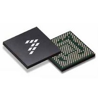
SC900841JVK Freescale Semiconductor, SC900841JVK Datasheet - Page 54

SC900841JVK
Manufacturer Part Number
SC900841JVK
Description
IC POWER MGT 338-MAPBGA
Manufacturer
Freescale Semiconductor
Specifications of SC900841JVK
Applications
PC's, PDA's
Operating Temperature
-40°C ~ 85°C
Mounting Type
Surface Mount
Package / Case
338-TBGA
Input Voltage
2.8 V to 4.4 V
Maximum Operating Temperature
+ 85 C
Minimum Operating Temperature
- 40 C
Lead Free Status / RoHS Status
Lead free / RoHS Compliant
Current - Supply
-
Voltage - Supply
-
Lead Free Status / Rohs Status
Lead free / RoHS Compliant
Available stocks
Company
Part Number
Manufacturer
Quantity
Price
Company:
Part Number:
SC900841JVK
Manufacturer:
Freescale Semiconductor
Quantity:
10 000
Company:
Part Number:
SC900841JVKR2
Manufacturer:
Freescale Semiconductor
Quantity:
10 000
Oscillator Specifications
conjunction with the Abracon™ ABS07-32.768KHZ-T or
equivalent, and is capable of handling its parametric
variations.
NDK™ NX2016AB-26MHZ SB1 or equivalent, and is capable
of handling its parametric variations.
Crystal oscillators are given in the Oscillator section on
Table 3
characteristics noted previously. The oscillator accuracy
depends largely on the temperature characteristics of the
used crystal. Application circuits can be optimized for
required accuracy by adapting the external crystal oscillator
network (via component accuracy and/or tuning).
Additionally, a clock calibration system is provided to adjust
the 32.768 cycle counter that generates the 1.0 Hz timer and
RTC registers; see
REAL TIME CLOCK (RTC)
year, month, and date, as well as daily alarm capabilities. The
real-time clock will use the 32.768 kHz oscillator as its input
clock. The real-time clock will be powered by the coin cell
backup battery as a last resort, if no other power source is
available (Battery or USB/Wall plug). The register set is
compatible with the Motorola™ MC146818 RTC device.
Overview
1.0 Hz clock for timekeeping. The seven time and calendar
registers keep track of seconds, minutes, hours, day-of-
week, day-of-month, month, and year. The three seconds,
minutes, and hours alarm registers can be used to generate
time-of-day alarm interrupts.
represented in 8-bit binary or BCD format. The hours and
hours alarm values can be represented in 24 hour or 12 hour
format, with AM/PM in the 12 hour mode. RTC control
register B allows for software configurable clock formatting
and interrupt masking. Control registers A, C, and D, report
software testable RTC status, including interrupt flags,
update-in-progress, and valid-RAM-time.
The clock and calendar registers will be initialized to
00:00:00, Sunday, January 1, 2000.
Features
• Counts seconds, minutes, and hours of the day
• Counts days of the week, date, month, and year
• Binary or BCD representation of time, calendar, and alarm
• 12 or 24 hour clock with AM and PM in 12 hour mode
• Automatic leap year compensation
54
900841
FUNCTIONAL DEVICE OPERATION
CLOCK GENERATION AND REAL TIME CLOCK (RTC)
The 32 kHz crystal oscillator has been optimized for use in
The 26 MHz is targeting for use in conjunction with the
The electrical characteristics of the 32 kHz and 26 MHz
The RTC block provides a real-time clock with time-of-day,
The RTC module uses a 15-bit counter to generate a
The RTC time, alarm, and calendar values can be
The RTC resets when the RTCPORB signal is driven low.
The RTC module includes the following features:
and
Table
4, taking into account the crystal
Real Time Clock (RTC)
for more detail.
• Automatic end of month recognition
• 15 bytes of clock, calendar, RTC control, and coin cell
• Two interrupts are separately software maskable and
• Time-of-day Alarm
• End-of-clock update cycle interrupt
• 15-bit counter to generate 1.0 Hz RTC clock
• Software testable Valid-ram-and-time status bit indicates
Modes of Operation
NORMAL MODE
calendar registers using the internal 1.0 Hz RTC clock. Once
per second, the alarm registers are compared to the current
time, and if enabled, an alarm interrupt will occur when the
alarm time matches the current time. During normal
operation, all 14 bytes of RTC and coin cell battery registers
can be read through the SPI interface. Control register B may
be updated to enable End-of-clock Update interrupts, alarm
interrupts, or to put the RTC in Set mode.
normal mode.
Coin Cell mode
continue to keep track of time using power provided by the
coin cell battery.
time, there is no read or write access to the RTC registers in
Coin Cell mode.
Set mode
suspended, and the software may update the time, calendar,
and alarm registers. The time and calendar formats must
match the formats specified by the DM and 12/24 format bits
in RTC register B. When the format bits are modified, all 14
time, calendar, and alarm registers must be updated in the
specified format.
Scan/Test mode
Setting the Time, Calendar, and Alarm
Register B should be set to a "1" to prevent time/calendar
updates from occurring. Select the data format by writing the
appropriate values to the DM and 24/12 bits in Register B.
and alarm locations in the format specified by Register B
(binary or BCD, 12 or 24 hour). All 10 time, calendar, and
registers
testable
data integrity
In Normal mode, the RTC module updates time and
The coin cell charger register is available for R/W in
When the application is powered down, the RTC will
Since the system SPI will be powered down during this
In Set mode, the clock and calendar updates are
Internal Test mode not available for the end application.
Before initializing the internal registers, the Set bit in
Next, the program should initialize all 10 time, calendar,
Analog Integrated Circuit Device Data
Freescale Semiconductor


