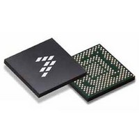
SC900841JVK Freescale Semiconductor, SC900841JVK Datasheet - Page 144

SC900841JVK
Manufacturer Part Number
SC900841JVK
Description
IC POWER MGT 338-MAPBGA
Manufacturer
Freescale Semiconductor
Specifications of SC900841JVK
Applications
PC's, PDA's
Operating Temperature
-40°C ~ 85°C
Mounting Type
Surface Mount
Package / Case
338-TBGA
Input Voltage
2.8 V to 4.4 V
Maximum Operating Temperature
+ 85 C
Minimum Operating Temperature
- 40 C
Lead Free Status / RoHS Status
Lead free / RoHS Compliant
Current - Supply
-
Voltage - Supply
-
Lead Free Status / Rohs Status
Lead free / RoHS Compliant
Available stocks
Company
Part Number
Manufacturer
Quantity
Price
Company:
Part Number:
SC900841JVK
Manufacturer:
Freescale Semiconductor
Quantity:
10 000
Company:
Part Number:
SC900841JVKR2
Manufacturer:
Freescale Semiconductor
Quantity:
10 000
- Current page: 144 of 192
- Download datasheet (8Mb)
AUDIO RECEIVE SECTION
Figure
GAIN CONTROL, MONO ADDER AND ROUTER
controlled in the programmable digital gain amplifiers. To
facilitate programming, independent settings are available for
the voice call and stereo audio use cases through
VDACVL[5:0], ADACVLR[5:0] and ADACVLL[5:0]
respectively. The gain of the feedback path of the digital
microphone can be set through DMICVLFB[5:0]. The gain of
the analog audio from RXINR and RXINL or pre-amplified
microphone inputs is controlled through the RAMPVLFB[5:0]
and LAMPVLFB[5:0] bits. All the gain settings have the same
granularity and range.
144
900841
FUNCTIONAL DEVICE OPERATION
AUDIO
Table 90. Receive Gain Control
Gain and Volume Setting Bits xxx[5:0]
The block diagram of the audio receive section is shown in
The gain of the digital audio in both left and right channels is
VINLSP L
SPP
SPM
LSPLP
LSPLM
GNDLSP L
VINLSP R
LSPRP
LSPRM
GNDLSP R
CPIN
HS L
CPC1
GNDCP
CPC2
HS R
CPOUT
RXOUTL
RXOUTR
72.
111001 (default)
Negative
Charge
Pump
000000
000001
…
Asp
Ahsl
Alspl
Alspr
Ahsr
Modulator
Class D
Stereo
Figure 72. Audio Receive Section Diagram
Gain
-57
-56
…
0
Units
Channel
Channel
dB
dB
dB
…
Mixer
Mixer
Right
Left
AMUTL, AMUTR bits. The muting of analog inputs is described
in the transmit section.
the transmit section can be mixed; the left channels and voice
DAC on the left channel mixer through MXLAUDL, MXLLINL,
and MXLMNDAC. The right channels and voice DAC on the
right channel mixer through MXRAUDR, MXRLINR, and
MXRMNDAC. The resulting mixed analog signal is routed to
the different output amplifiers.
EAR PIECE SPEAKER AMPLIFIER ASP
which drives the ear piece of the application in a bridge tied
load configuration. The amplifier is supplied from the battery
3
3
Table 90. Receive Gain Control
The signal paths can be muted through the VMUTL,
The analog signal from the stereo DAC, the voice DAC, and
The left channel audio can be routed to the Asp amplifier,
111110
111111
…
D to A
Wideband Stereo D to A
D to A
D to A
14bit
16bit
16bit
Voice Codec D to A
Analog Integrated Circuit Device Data
-57dB to +6dB
1dB Steps
-57dB to +6dB
-57dB to +6dB
-57dB to +6dB
1dB Steps
1dB Steps
1dB Steps
Arxr
Arxl
Freescale Semiconductor
Transmit Section
-57dB to +6dB
Sidetone
1dB Steps
+5
+6
…
From
+
Transmit Section
Digital Interface
RX Voice
RX Left
RX Right
TXINR
TXINL
From
From
dB
dB
…
Related parts for SC900841JVK
Image
Part Number
Description
Manufacturer
Datasheet
Request
R
Part Number:
Description:
Manufacturer:
Freescale Semiconductor, Inc
Datasheet:
Part Number:
Description:
Manufacturer:
Freescale Semiconductor, Inc
Datasheet:
Part Number:
Description:
Manufacturer:
Freescale Semiconductor, Inc
Datasheet:
Part Number:
Description:
Manufacturer:
Freescale Semiconductor, Inc
Datasheet:
Part Number:
Description:
Manufacturer:
Freescale Semiconductor, Inc
Datasheet:
Part Number:
Description:
Manufacturer:
Freescale Semiconductor, Inc
Datasheet:
Part Number:
Description:
Manufacturer:
Freescale Semiconductor, Inc
Datasheet:
Part Number:
Description:
Manufacturer:
Freescale Semiconductor, Inc
Datasheet:
Part Number:
Description:
Manufacturer:
Freescale Semiconductor, Inc
Datasheet:
Part Number:
Description:
Manufacturer:
Freescale Semiconductor, Inc
Datasheet:
Part Number:
Description:
Manufacturer:
Freescale Semiconductor, Inc
Datasheet:
Part Number:
Description:
Manufacturer:
Freescale Semiconductor, Inc
Datasheet:
Part Number:
Description:
Manufacturer:
Freescale Semiconductor, Inc
Datasheet:
Part Number:
Description:
Manufacturer:
Freescale Semiconductor, Inc
Datasheet:
Part Number:
Description:
Manufacturer:
Freescale Semiconductor, Inc
Datasheet:


