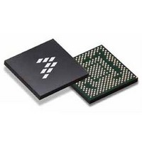
SC900841JVK Freescale Semiconductor, SC900841JVK Datasheet - Page 117

SC900841JVK
Manufacturer Part Number
SC900841JVK
Description
IC POWER MGT 338-MAPBGA
Manufacturer
Freescale Semiconductor
Specifications of SC900841JVK
Applications
PC's, PDA's
Operating Temperature
-40°C ~ 85°C
Mounting Type
Surface Mount
Package / Case
338-TBGA
Input Voltage
2.8 V to 4.4 V
Maximum Operating Temperature
+ 85 C
Minimum Operating Temperature
- 40 C
Lead Free Status / RoHS Status
Lead free / RoHS Compliant
Current - Supply
-
Voltage - Supply
-
Lead Free Status / Rohs Status
Lead free / RoHS Compliant
Available stocks
Company
Part Number
Manufacturer
Quantity
Price
Company:
Part Number:
SC900841JVK
Manufacturer:
Freescale Semiconductor
Quantity:
10 000
Company:
Part Number:
SC900841JVKR2
Manufacturer:
Freescale Semiconductor
Quantity:
10 000
- Current page: 117 of 192
- Download datasheet (8Mb)
Table 75. Signaling /Status LED Driver Register and Bit Description
setting. If a PWM change is programmed via the SPI when the
LEDxRAMP=0, then the change is immediate rather than
spread out over a PWM sweep.
the color mixing should be obtained by the current level setting
so that the intensity is set through the PWM duty cycle. In
addition, programmable blink rates are provided. Blinking is
obtained by lowering the PWM repetition rate of each of the
drivers through LEDxBLNK[1:0] while the on period is
determined by the duty cycle setting, default is 0.5 s ON time.
To avoid high frequency spur coupling in the application, the
Analog Integrated Circuit Device Data
Freescale Semiconductor
For color mixing and in order to guarantee a constant color,
LED0BLNK
LED1BLNK
LED2BLNK
LED0BRT
LED1BRT
LED2BRT
LED3BRT
Name
Bits
1:0
3:2
5:4
7:6
1:0
3:2
5:4
LEDR1 Driver Current Settings
x0 = 0 mA
x1 = 8.0 mA
x2 = 20 mA
x3 = 28 mA
LEDR1 Blink Setting, with a default on time of 0.5 s
x0 = No Blink
x1 = 1.0 s
x2 = 4.0 s
x3 = 8.0 s
LEDG1 Driver Current Settings
x0 = 0 mA
x1 = 8.0 mA
x2 = 20 mA
x3 = 28 mA
LEDG1 Blink Setting, with a default on time of 0.5 s
x0 = No Blink
x1 = 1.0 s
x2 = 4.0 s
x3 = 8.0 s
LEDB1 Driver Current Settings
x0 = 0 mA
x1 = 8.0 mA
x2 = 20 mA
x3 = 28 mA
LEDB1 Blink Setting, with a default on time of 0.5 s
x0 = No Blink
x1 = 1.0 s
x2 = 4.0 s
x3 = 8.0 s
LEDR2 Driver Current Settings
x0 = 0 mA
x1 = 8.0 mA
x2 = 20 mA
x3 = 28 mA
LEDBRT0 (ADDR 0x25 - R/W - Default Value: 0x00)
LEDBRT1 (ADDR 0x26 - R/W - Default Value: 0x00)
switching edges of the output drivers are softened. During
blinking, so LEDxBLNK[1:0] is not "00", ramping and dimming
patterns cannot be applied.
LEDs they can also be used as general purpose open drain
outputs for logic signaling or as generic PWM generator
outputs. For the maximum voltage ratings see
Ratings.
Signaling/Status LED Drivers Status/Control Registers
and Bits Description
Apart from using the signal/status LED drivers for driving
Description
FUNCTIONAL DEVICE OPERATION
LIGHTING SYSTEM
Maximum
900841
117
Related parts for SC900841JVK
Image
Part Number
Description
Manufacturer
Datasheet
Request
R
Part Number:
Description:
Manufacturer:
Freescale Semiconductor, Inc
Datasheet:
Part Number:
Description:
Manufacturer:
Freescale Semiconductor, Inc
Datasheet:
Part Number:
Description:
Manufacturer:
Freescale Semiconductor, Inc
Datasheet:
Part Number:
Description:
Manufacturer:
Freescale Semiconductor, Inc
Datasheet:
Part Number:
Description:
Manufacturer:
Freescale Semiconductor, Inc
Datasheet:
Part Number:
Description:
Manufacturer:
Freescale Semiconductor, Inc
Datasheet:
Part Number:
Description:
Manufacturer:
Freescale Semiconductor, Inc
Datasheet:
Part Number:
Description:
Manufacturer:
Freescale Semiconductor, Inc
Datasheet:
Part Number:
Description:
Manufacturer:
Freescale Semiconductor, Inc
Datasheet:
Part Number:
Description:
Manufacturer:
Freescale Semiconductor, Inc
Datasheet:
Part Number:
Description:
Manufacturer:
Freescale Semiconductor, Inc
Datasheet:
Part Number:
Description:
Manufacturer:
Freescale Semiconductor, Inc
Datasheet:
Part Number:
Description:
Manufacturer:
Freescale Semiconductor, Inc
Datasheet:
Part Number:
Description:
Manufacturer:
Freescale Semiconductor, Inc
Datasheet:
Part Number:
Description:
Manufacturer:
Freescale Semiconductor, Inc
Datasheet:


