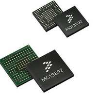
MC13892BJVL Freescale Semiconductor, MC13892BJVL Datasheet - Page 85

MC13892BJVL
Manufacturer Part Number
MC13892BJVL
Description
IC PMU I.MX51/37/35/27 186MAPBGA
Manufacturer
Freescale Semiconductor
Datasheets
1.MC13892AJVLR2.pdf
(156 pages)
2.MC13892AJVLR2.pdf
(2 pages)
3.MC13892AJVLR2.pdf
(16 pages)
4.MC13892AJVLR2.pdf
(5 pages)
Specifications of MC13892BJVL
Applications
Battery Management, Display (LED Drivers), Handheld/Mobile Devices, Power Supply
Operating Temperature
-40°C ~ 85°C
Mounting Type
Surface Mount
Package / Case
186-LFBGA
Mounting Style
SMD/SMT
Duty Cycle (max)
55 %
Input Voltage
- 0.3 V to + 20 V
Maximum Operating Temperature
+ 85 C
Minimum Operating Temperature
- 30 C
Output Current
30 mA
Output Voltage
3.3 V
Topology
Boost
Lead Free Status / RoHS Status
Lead free / RoHS Compliant
Current - Supply
-
Voltage - Supply
-
Lead Free Status / Rohs Status
Lead free / RoHS Compliant
Available stocks
Company
Part Number
Manufacturer
Quantity
Price
Company:
Part Number:
MC13892BJVL
Manufacturer:
Freescale Semiconductor
Quantity:
10 000
Company:
Part Number:
MC13892BJVLR2
Manufacturer:
Freescale Semiconductor
Quantity:
10 000
BP and output settings. For stability reasons a small minimum ESR may be required. In the Low Power mode for VVIDEO an
internal bypass path is used instead of the external PNP. External PNP devices are always to be connected to the BP line in the
application. The recommended PNP device is the ON Semiconductor NSS12100XV6T1G which is capable of handling up to
250mW of continuous dissipation at minimum footprint and 75 °C of ambient. For use cases where up to 500mW of dissipation
is required, the recommended PNP device is the ON Semiconductor™ NSS12100UW3TCG. For stability reasons a small
minimum ESR may be required.
LOW VOLTAGE SUPPLIES
peripheral needs. Depending on the lineup and power requirements, these supplies may be considered for sharing with other
loads, but noise injection must be avoided and filtering added if necessary, to ensure suitable PLL performance. The VDIG and
VPLL regulators have a dedicated input supply pin: VINDIG for the VDIG regulator, and VINPLL for the VPLL regulator. VINDIG
and VINPLL can be connected to either BP or a 1.8V switched mode power supply rail, such as from SW4 for the two lower set
points of each regulator VPLL[1:0] and VDIG[1:0] = [00], [01]. In addition, when the two upper set points are used VPLL[1:0] and
VDIG[1:0] = [10], [11], the inputs (VINDIG and VINPLL) can be connected to either BP of a 2.2 V nominal external switched mode
power supply rail to improve power dissipation.
PERIPHERAL INTERFACING
peripherals at SPIVCC level (powered from SW4), and a higher voltage interface level associated with other peripherals not
compatible with the 1.8 V SPIVCC. VIOHI is provided at a fixed 2.775 V level for such interfaces, and may also be applied to
other system needs within the guidelines of the regulator specifications. The input VINIOHI is not only used by the VIOHI
regulator, but also by other blocks, therefore it should always be connected to BP, even if the VIOHI regulator is not used by the
system.
CAMERA
other parts of the system, as well as to select from a number of VCAM output levels for camera vendor flexibility. In applications
Analog Integrated Circuit Device Data
Freescale Semiconductor
An external PNP is utilized for VVIDEO to avoid excess on-chip power dissipation at high loads, and large differential between
VAUDIO is implemented with an integrated PMOS pass FET and has a dedicated input supply pin VINAUDIO.
The following tables contain the specifications for the VVIDEO, VAUDIO.
VDIG and VPLL are provided for isolated biasing of the Baseband system PLLs for clock generation in support of protocol and
IC interfaces in the lineups generally fall in two categories: low voltage IO primarily associated with the AP IC and certain
VIOHI has an internal PMOS pass FET which will support loads up to 100 mA.
The camera module is supplied by the regulator VCAM. This allows powering the entire module independent of the rest of
Table 55. VPLL and VDIG Voltage Control
Parameter
VPLL[1:0]
VDIG[1:0]
Table 54. VVIDEO and VAUDIO Voltage Control
VVIDEO
VAUDIO
Parameter
Value
00
01
10
11
00
01
10
11
Value
output = 1.2 V
output = 1.25 V
output = 1.5 V
output = 1.8 V
output = 1.05 V
output = 1.25 V
output = 1.65 V
output = 1.8 V
00
01
10
00
01
10
11
11
Function
Output = 2.700 V
Output = 2.775 V
Output = 2.500 V
Output = 2.600 V
Output = 2.300 V
Output = 2.500 V
Output = 2.775 V
Output = 3.000 V
Function
ILoad max
50 mA
50 mA
50 mA
50 mA
50 mA
50 mA
50 mA
50 mA
250 mA / 350 mA
250 mA / 350 mA
250 mA / 350 mA
250 mA / 350 mA
150 mA
150 mA
150 mA
150 mA
BP or 1.8 V
BP or 1.8 V
BP or External Switcher
BP or External Switcher
BP or 1.8 V
BP or 1.8 V
BP or External Switcher
BP or External Switcher
ILoad max
Input Supply
FUNCTIONAL DEVICE OPERATION
SUPPLIES
13892
85


