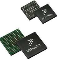
MC13892BJVL Freescale Semiconductor, MC13892BJVL Datasheet - Page 32

MC13892BJVL
Manufacturer Part Number
MC13892BJVL
Description
IC PMU I.MX51/37/35/27 186MAPBGA
Manufacturer
Freescale Semiconductor
Datasheets
1.MC13892AJVLR2.pdf
(156 pages)
2.MC13892AJVLR2.pdf
(2 pages)
3.MC13892AJVLR2.pdf
(16 pages)
4.MC13892AJVLR2.pdf
(5 pages)
Specifications of MC13892BJVL
Applications
Battery Management, Display (LED Drivers), Handheld/Mobile Devices, Power Supply
Operating Temperature
-40°C ~ 85°C
Mounting Type
Surface Mount
Package / Case
186-LFBGA
Mounting Style
SMD/SMT
Duty Cycle (max)
55 %
Input Voltage
- 0.3 V to + 20 V
Maximum Operating Temperature
+ 85 C
Minimum Operating Temperature
- 30 C
Output Current
30 mA
Output Voltage
3.3 V
Topology
Boost
Lead Free Status / RoHS Status
Lead free / RoHS Compliant
Current - Supply
-
Voltage - Supply
-
Lead Free Status / Rohs Status
Lead free / RoHS Compliant
Available stocks
Company
Part Number
Manufacturer
Quantity
Price
Company:
Part Number:
MC13892BJVL
Manufacturer:
Freescale Semiconductor
Quantity:
10 000
Company:
Part Number:
MC13892BJVLR2
Manufacturer:
Freescale Semiconductor
Quantity:
10 000
FUNCTIONAL DESCRIPTION
FUNCTIONAL PIN DESCRIPTION
CHARGER
CHRGRAW
in cases where the charger is being supplied from the USB cable. The minimum voltage for this pin depends on BATTMIN
threshold value (see
the accessory via the CHRGRAW pin. To accomplish this, the charger needs to be configured in reverse supply mode.
CHRGCTRL1
CHRGCTRL2
CHRGISNS
sense resistor connected between CHRGISNS and BPSNS.
BPSNS
sense resistor. This resistor is connected between CHRGISNS and BPSNS.
BP
through an ADC at this pin.
BATTFET
be floating.
BATTISNS
voltage drop over the sense resistor between BATT and BATTISNS.
BATT
pin. The current flowing out of and into the battery can be read via the ADC by monitoring the voltage drop over the sense resistor
between BATT and BATTISNS.
BATTISNSCC
directly to the 0.020 Ω sense resistor via a separate route from BATTISNS. The coulomb counter monitors the current flowing in/
out of the battery by integrating the voltage drop over the BATTISNCC and the BATT pin.
32
13892
1. Charger input. The charger voltage is measured through an ADC at this pin. The UVBUS pin must be shorted to CHRGRAW
2. Output to battery supplied accessories. The battery voltage can be applied to an accessory by enabling the charge path for
Driver output for charger path FET M1.
Driver output for charger path FET M2.
Charge current sensing point 1. The charge current is read by monitoring the voltage drop over the charge current 100 mΩ
1. BP sense point. BP voltage is sensed at this pin and compared with the voltage at CHRGRAW.
2. Charge current sensing point 2. The charge current is read by monitoring the voltage drop over the charge current 100 mΩ
This pin is the application supply point, the input supply to the IC core circuitry. The application supply voltage is sensed
Driver output for battery path FET M3. If no charging system is required or single path is implemented, the pin BATTFET must
Battery current sensing point 1. The current flowing out of and into the battery can be read via the ADC by monitoring the
Battery positive terminal. Battery current sensing point 2. The supply voltage of the battery is sensed through an ADC on this
Accumulated current counter current sensing point. This is the coulomb counter current sense point. It should be connected
Battery Interface and
FUNCTIONAL PIN DESCRIPTION
Control).
FUNCTIONAL DESCRIPTION
Analog Integrated Circuit Device Data
Freescale Semiconductor


