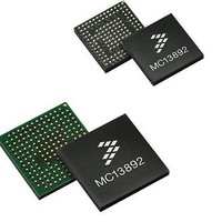
MC13892BJVL Freescale Semiconductor, MC13892BJVL Datasheet - Page 72

MC13892BJVL
Manufacturer Part Number
MC13892BJVL
Description
IC PMU I.MX51/37/35/27 186MAPBGA
Manufacturer
Freescale Semiconductor
Datasheets
1.MC13892AJVLR2.pdf
(156 pages)
2.MC13892AJVLR2.pdf
(2 pages)
3.MC13892AJVLR2.pdf
(16 pages)
4.MC13892AJVLR2.pdf
(5 pages)
Specifications of MC13892BJVL
Applications
Battery Management, Display (LED Drivers), Handheld/Mobile Devices, Power Supply
Operating Temperature
-40°C ~ 85°C
Mounting Type
Surface Mount
Package / Case
186-LFBGA
Mounting Style
SMD/SMT
Duty Cycle (max)
55 %
Input Voltage
- 0.3 V to + 20 V
Maximum Operating Temperature
+ 85 C
Minimum Operating Temperature
- 30 C
Output Current
30 mA
Output Voltage
3.3 V
Topology
Boost
Lead Free Status / RoHS Status
Lead free / RoHS Compliant
Current - Supply
-
Voltage - Supply
-
Lead Free Status / Rohs Status
Lead free / RoHS Compliant
Available stocks
Company
Part Number
Manufacturer
Quantity
Price
Company:
Part Number:
MC13892BJVL
Manufacturer:
Freescale Semiconductor
Quantity:
10 000
Company:
Part Number:
MC13892BJVLR2
Manufacturer:
Freescale Semiconductor
Quantity:
10 000
FUNCTIONAL DEVICE OPERATION
SUPPLIES
Table 43. Power Tree Summary
BUCK SWITCHER SUPPLIES
and SW2 are used for supplying the application processor core power domains. Split power domains allow independent DVS
control for processor power optimization, or to support technologies with a mix of device types with different voltage ratings. SW3
is used for powering internal processor memory as well as low voltage peripheral devices and interfaces which can run at the
same voltage level. SW4 is used for powering external memory as well as low voltage peripheral devices and interfaces which
can run at the same voltage level.
direct interfacing without bandwidth limiting synchronizers.
(when present).
72
13892
VCAM
VGEN1
VGEN2
VGEN3
VUSB
Four buck switchers are provided with integrated power switches and synchronous rectification. In a typical application, SW1
An anticipated platform use case applies SW1 and SW2 to processor power domains that require voltage alignment to allow
The buck switchers have to be supplied from the system supply BP, which is drawn from the main battery or the battery charger
Supply
Camera supply, internal PMOS
Camera supply, external PNP
General peripherals supply #1, external PNP
General peripherals supply #2, external PNP
General peripherals supply #3, internal PMOS
General peripherals supply #3, external PNP
USB Transceiver supply
Figure 16
Purpose (Typical Application)
shows a high level block diagram of the buck switchers.
Figure 16. Buck Switcher Architecture
2.5/2.6/2.75/3.0
2.5/2.6/2.75/3.0
1.2/1.5/2.775/3.15
1.2/1.5/1.6/1.8/2.7/2.8/3.0/3.15
1.8/2.9
1.8/2.9
3.3
Output Voltage (in V)
Analog Integrated Circuit Device Data
Freescale Semiconductor
Load Capability (in mA)
250
200
350
250
100
65
50


