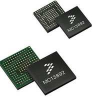
MC13892BJVL Freescale Semiconductor, MC13892BJVL Datasheet - Page 73

MC13892BJVL
Manufacturer Part Number
MC13892BJVL
Description
IC PMU I.MX51/37/35/27 186MAPBGA
Manufacturer
Freescale Semiconductor
Datasheets
1.MC13892AJVLR2.pdf
(156 pages)
2.MC13892AJVLR2.pdf
(2 pages)
3.MC13892AJVLR2.pdf
(16 pages)
4.MC13892AJVLR2.pdf
(5 pages)
Specifications of MC13892BJVL
Applications
Battery Management, Display (LED Drivers), Handheld/Mobile Devices, Power Supply
Operating Temperature
-40°C ~ 85°C
Mounting Type
Surface Mount
Package / Case
186-LFBGA
Mounting Style
SMD/SMT
Duty Cycle (max)
55 %
Input Voltage
- 0.3 V to + 20 V
Maximum Operating Temperature
+ 85 C
Minimum Operating Temperature
- 30 C
Output Current
30 mA
Output Voltage
3.3 V
Topology
Boost
Lead Free Status / RoHS Status
Lead free / RoHS Compliant
Current - Supply
-
Voltage - Supply
-
Lead Free Status / Rohs Status
Lead free / RoHS Compliant
Available stocks
Company
Part Number
Manufacturer
Quantity
Price
Company:
Part Number:
MC13892BJVL
Manufacturer:
Freescale Semiconductor
Quantity:
10 000
Company:
Part Number:
MC13892BJVLR2
Manufacturer:
Freescale Semiconductor
Quantity:
10 000
the chip as a low ohmic FET. The placement of an external diode is therefore not required, but overall switcher efficiency may
benefit from this. The buck converters permit a 100% duty cycle operation.
synchronous PWM control is the most efficient, while maintaining a constant switching frequency. Two PWM modes are
available: the first mode sacrifices low load efficiency for a continuous switching operation (PWM-NPS). The second mode offers
better low load efficiency by allowing the absence of switching cycles at low output loading (PWM-PS). This pulse skipping
feature improves efficiency by reducing dynamic switching losses by simply switching less often.
control scheme. The frequency spectrum in this case will be a function of input and output voltage, loading, and the external
components. Due to its spectral variance and lighter drive capability, PFM mode is generally reserved for non-active radio modes
and Deep Sleep operation.
Switchers section in
stands for 1, 2, 3, or 4 (i.e., SWx = SW1, SW2, SW3, and SW4).
with SWxHI for SW2, SW3, and SW4 bucks, SW1 is limited to only one output range. Presets are available for both the Normal
and Standby operation. SW1 and SW2 also include pin controlled DVS operation. When transitioning from one voltage to
another, the output voltage slope is controlled in steps of 25 mV per time step (time step as defined for DVS stepping for SW1
and SW2, fixed at 4.0 μs for SW3 and SW4). This allows for support of dynamic voltage scaling (DVS) by using SPI driven voltage
steps, state machine defined modes, and direct DVSx pin control.
the inrush current at startup. A built-in current limiter ensures that during normal operation, the maximum current through the coil
is not exceeded. This current limiter can be disabled by setting the SWILIMB bit.
SWITCHING FREQUENCY
upon the 32.768 kHz oscillator signal by multiplying it by 96. To reduce spurious radio channels, the PLL can be programmed
via PLLX[2:0] to different values as shown in
PLL clock signal is not needed elsewhere in the system. The clocking system provides nearly instantaneously, a high frequency
clock to the switchers when the switchers are activated or exit the PFM mode for PWM mode. The PLL can be configured for
continuous operation by setting the SPI bit PLLEN = 1.
Analog Integrated Circuit Device Data
Freescale Semiconductor
The Buck switcher topology includes an integrated synchronous rectifier, meaning that the rectifying diode is implemented on
During normal operation, several power modes are possible depending on the loading. For medium and full loading,
In its lowest power mode, the switcher can regulate using hysteresis control known as a Pulse Frequency Modulation (PFM)
Buck modes of operation are programmable for explicitly defined or load-dependent control (Adaptive). Refer to the Buck
Common control bits available to each buck regulator may be designated with a suffix “x” within this specification, where x
The output voltages of the buck switchers are SPI configurable, and two output ranges are available, individually programmed
When initially activated, switcher outputs will apply controlled stepping to the programmed value. The soft start feature limits
Point of Load feedback is intended for minimizing errors due to board level IR drops.
The switchers are driven by a high frequency clock. By default, the PLL generates an effective 3.145728 MHz signal based
To reduce overall current drain, the PLL is automatically turned off if all switchers are in a PFM mode or turned off, and if the
Power Control System
Table 44. PLL Multiplication Factor
PLLX[2:0]
100 (default)
000
001
010
011
101
110
111
for details.
Table
44.
Multiplication
Factor
102
105
84
87
90
93
96
99
Switching Frequency (Hz)
2 752 512
2 850 816
2 949 120
3 047 424
3 145 728
3 244 032
3 342 336
3 440 640
FUNCTIONAL DEVICE OPERATION
SUPPLIES
13892
73


