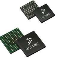
MC13892BJVL Freescale Semiconductor, MC13892BJVL Datasheet - Page 42

MC13892BJVL
Manufacturer Part Number
MC13892BJVL
Description
IC PMU I.MX51/37/35/27 186MAPBGA
Manufacturer
Freescale Semiconductor
Datasheets
1.MC13892AJVLR2.pdf
(156 pages)
2.MC13892AJVLR2.pdf
(2 pages)
3.MC13892AJVLR2.pdf
(16 pages)
4.MC13892AJVLR2.pdf
(5 pages)
Specifications of MC13892BJVL
Applications
Battery Management, Display (LED Drivers), Handheld/Mobile Devices, Power Supply
Operating Temperature
-40°C ~ 85°C
Mounting Type
Surface Mount
Package / Case
186-LFBGA
Mounting Style
SMD/SMT
Duty Cycle (max)
55 %
Input Voltage
- 0.3 V to + 20 V
Maximum Operating Temperature
+ 85 C
Minimum Operating Temperature
- 30 C
Output Current
30 mA
Output Voltage
3.3 V
Topology
Boost
Lead Free Status / RoHS Status
Lead free / RoHS Compliant
Current - Supply
-
Voltage - Supply
-
Lead Free Status / Rohs Status
Lead free / RoHS Compliant
Available stocks
Company
Part Number
Manufacturer
Quantity
Price
Company:
Part Number:
MC13892BJVL
Manufacturer:
Freescale Semiconductor
Quantity:
10 000
Company:
Part Number:
MC13892BJVLR2
Manufacturer:
Freescale Semiconductor
Quantity:
10 000
FUNCTIONAL DEVICE OPERATION
PROGRAMMABILITY
SPI INTERFACE DESCRIPTION
field. In addition, there is one “dead” bit between the data and address fields. The remaining bits include 6 address bits to address
the 64 data fields and one write enable bit to select whether the SPI transaction is a read or a write.
write bit if this is to be a read command only.
go active again. The MISO line will be tri-stated while CS is low.
SPI sequence.
42
13892
Table 8. Register Set
15
12
13
14
The SPI interface is comprised of the package pins listed in
The control bits are organized into 64 fields. Each of these 64 fields contains 32 bits. A maximum of 24 data bits are used per
The register set will be to a large extent compatible with the MC13783 in order to facilitate software development.
For each SPI transfer, first a one is written to the read/write bit if this SPI transfer is to be a write. A zero is written to the read/
The CS line must remain high during the entire SPI transfer. To start a new SPI transfer, the CS line must go inactive and then
To read a field of data, the MISO pin will output the data field pointed to by the 6 address bits loaded at the beginning of the
Unused
Power Control 0
Power Control 1
Power Control 2
Table 9. SPI Interface Pin Description
Register
CLK
MOSI
MISO
CS
INT
SPIVCC
Interrupt
SPI Bus
Supply
Clock input line, data shifting occurs at the rising edge
Serial data input line
Serial data output line
Clock enable line, active high
Interrupt to processor
Processor SPI bus supply
Figure 5. SPI Transfer Protocol Single Read/Write Access
28
29
30
31
Switchers 4
Switchers 5
Regulator Setting 0
Regulator Setting 1
Register
Table
44
45
46
47
Description
Description
Description
9.
ADC 1
ADC 2
ADC 3
ADC4
Register
Analog Integrated Circuit Device Data
60
61
62
63
Freescale Semiconductor
Test 1
Test 2
Test 3
Test 4
Register


